Author: Addithive

  • Additive Manufacturing is No Longer the Future

    Additive Manufacturing is No Longer the Future

    It’s the Engine of Industrial Transformation

    By mid-2025, additive manufacturing (AM) has broken out of the prototyping corner and taken center stage as a pillar of Industry 4.0. With a global market value projected to soar from $20.37 billion in 2023 to $88.28 billion by 2030, at a staggering 23.3% CAGR, AM is no longer an emerging technology—it is a strategic enabler of design freedom, supply chain resilience, and sustainable production.

    What’s driving this explosive trajectory? A potent mix of next-generation hardware, novel material breakthroughs, automation-first workflows, and globally coordinated regulatory frameworks. And yet, for all its promise, AM’s future hinges on our ability to scale precision, ensure repeatability, and harmonize standards. This article unpacks the current state and near-future outlook for additive manufacturing through three pivotal lenses: technological innovation, regulatory evolution, and regional momentum.


    From Prototype to Production – How Next-Gen Additive Technologies Are Breaking Barriers

    “From five-micron tolerance to decentralized, high-volume output, AM is reinventing how we think about manufacturing itself.”

    By 2025, the range and maturity of AM technologies have expanded dramatically. Innovations now span nearly every corner of the additive toolbox, each solving a specific pain point in the production chain:

    🔧 Precision and Performance

    High-resolution powder bed fusion systems like Aixway3D’s Precision-100 deliver tolerances as tight as 2–5 microns, enabling aerospace-grade parts with minimal post-processing. Meanwhile, selective laser sintering (SLS) solutions from 3DPS now hit 1 mm wall thickness with 0.2 mm precision—capabilities critical for functional parts in aerospace and healthcare.

    Additive manufacturing machine with a control panel, a screen, and various components designed for precision 3D printing.
    https://aixway3d.de

    🤖 Automation and Scaling

    Automation has moved from vision to implementation. AM-Flow’s robotic workflows and Printinue’s continuous production loops allow fully digitized, lights-out manufacturing. These systems aren’t just cost savers—they’re the scaffolding for decentralized, on-demand production hubs.

    🧪 Material Science at the Forefront

    Sustainability and performance are converging. f3nice is commercializing recycled metal powders, while Foundation Alloy focuses on high-performance, application-specific metals. In the polymer world, RAYSHAPE’s DLP machines and NematX’s liquid crystal polymers (LCP) are redefining precision and durability.

    🧬 Biological Integration

    Bioprinting is transitioning from lab experiment to clinical pilot. Brinter’s modular bioprinters are enabling scaffold fabrication for tissue engineering, while medical-grade resins are entering the DLP mainstream thanks to Boston Micro Fabrication.

    🏭 High-Volume Breakthroughs

    Q.big 3D’s QUEEN 1 introduces Volumetric Filament Grid Fusion (VFGF), enabling affordable large-part production. Pair this with Phasio’s decentralized manufacturing software, and the result is an elastic production model, ready for reshoring supply chains.

    A modern 3D printer, labeled 'QUEEN 1' by Q.big 3D, designed for high-volume additive manufacturing, featuring a sleek black and white exterior.
    https://www.qbig3d.de/

    Yet, for all the progress, challenges persist: throughput in metal AM remains relatively low; material costs are still high for certain alloys and biocompatible resins; and post-processing—though improving—is often the bottleneck in full-stack workflows.


    The Rules Are Changing – Regulation, Standardization, and Safety in a Maturing Ecosystem

    “AM’s growth is as much about digital lasers as it is about legal lines.”

    As additive manufacturing moves into regulated industries—healthcare, aerospace, defense—the rulebook is expanding fast. The real story of 2025 isn’t just what we can print, but what we’re allowed to.

    the word compliance written in scrabble letters

    🧭 Healthcare: Navigating FDA Waters

    The U.S. FDA’s framework for additive medical devices demands rigorous testing on porosity, mechanical integrity, and traceability. While this ensures patient safety, smaller companies often face steep regulatory and cost barriers. Quality assurance software, in-situ monitoring, and ISO-aligned certification programs are becoming baseline requirements.

    ✈ Aerospace & Safety Protocols

    The EN ISO/ASTM 52938-1 standard in Europe now governs laser beam and powder machine safety, with ISO/ASTM 52931 setting the groundwork for metallic material properties. These standards are essential—but introduce a lag between tech innovation and regulatory acceptance. The result? Slower integration of novel materials in high-stakes use cases.

    🧠 Intellectual Property in a Digital World

    2025 IP landscape is shifting. With digital inventories and mass customization, we’re entering an era of design ownership complexity. Licensing platforms and blockchain verification may offer the next frontier in securing AM intellectual property.

    🔒 Sector-Specific Limits: Formula 1 & Defense

    Regulation isn’t always enabling. Formula 1’s 2026 technical guidelines now limit AM for critical components like heat exchangers—highlighting how even proven technologies can be gated when safety margins are razor-thin.

    So what’s the path forward? Ongoing standardization and government-supported certification labs—like those seen in India and the U.S.—are helping harmonize global frameworks. But until regulations match innovation speed, AM will need to navigate cautiously through fragmented compliance landscapes.


    Around the World in 3D – Regional Powerhouses and National Strategies

    “In the global AM race, innovation is local—but ambition is universal.”

    The geographic spread of additive manufacturing tells a compelling story: while the technology is global, its development is deeply regional. Each powerhouse has distinct goals, advantages, and policy frameworks.

    close up of globe

    🇺🇸 North America – Defense, Healthcare, and Private Capital

    With >34% global market share, the U.S. leads in AM R&D and deployment. Initiatives like America Makes and NIST’s metrology efforts drive certification and workforce development. The sector thrives on defense and aerospace demand, bolstered by deep venture capital pools (over $600M in VC funding in 2018 alone).

    🇪🇺 Europe – Innovation Through Standardization

    Home to EOS, Materialise, and Voxeljet, Europe’s AM leadership rests on strong public-private R&D. EU initiatives fund sustainability-focused programs, while standardization bodies build the backbone for cross-border interoperability.

    🇮🇳 India – AM as a Strategic Leapfrog

    India’s 2022 National Strategy set bold goals: 100 startups, 100,000 trained workers, and 50 certified AM products by 2025. With Atal Tinkering Labs and seven state-funded AM centers, India is fast-tracking homegrown innovation. Healthcare and tooling are immediate beneficiaries.

    🇨🇳 China – Industrialization and Scale

    Though detailed 2025 stats were lacking, policy momentum points to AM’s central role in China’s manufacturing modernization. With strengths in automotive and consumer electronics, China’s scale advantage and national industrial policies make it a formidable player.

    Regional insights also reveal who’s betting big on decentralized manufacturing. For instance, India’s state-level partnerships and U.S. startups using Phasio’s cloud-driven tools point toward a future of “digital-first factories”—where agility, not just output, defines competitiveness.


    The Next Five Years Will Redefine What We Call a Factory

    Additive manufacturing in 2025 isn’t a novelty—it’s a necessity. As supply chains de-risk, as sustainability moves from CSR to ROI, and as engineers demand more from geometry and performance, AM answers the call.

    But the real transformation lies ahead. From 2025 to 2030, we’ll likely see:

    • Cost parity with traditional methods through high-throughput and automated workflows
    • Explosive material diversity, including bioresorbable implants and aerospace-grade recycled alloys
    • Mainstream adoption of hybrid AM-CNC lines for mass customization
    • Wider use of digital inventories, fundamentally changing spare parts and MRO economics


    If you’re leading innovation in engineering or manufacturing, now is the time to ask: Is your product portfolio designed for AM? Are your teams trained in DfAM principles? Are your suppliers AM-capable?

    The next industrial leap won’t be won by those who wait for standards to stabilize or costs to drop—it will be led by those who experiment, partner, and evolve with the technology.

    The additive future is not just being built. It’s being printed—one micron at a time.


    Technical Terms:

    • AM – Additive Manufacturing
    • PBF – Powder Bed Fusion
    • SLS – Selective Laser Sintering
    • DLP – Digital Light Processing
    • LCP – Liquid Crystal Polymer
    • VFGF – Volumetric Filament Grid Fusion
    • FDM – Fused Deposition Modeling
    • WAAM – Wire Arc Additive Manufacturing
    • DED – Direct Energy Deposition

    Design and Process Frameworks:

    • DfAM – Design for Additive Manufacturing
    • TRL – Technology Readiness Level
    • CAD – Computer-Aided Design

    Standards and Regulatory Bodies:

    • EN ISO/ASTM 52938-1 – European/International Standard for Safety in Laser-Based Additive Manufacturing Machines
    • ISO/ASTM 52931 – Standard for Metallic Materials in Additive Manufacturing
    • FDA – Food and Drug Administration
    • NIST – National Institute of Standards and Technology

    Organizations and Initiatives:

    • R\&D – Research and Development
    • VC – Venture Capital
    • IP – Intellectual Property

    📚 Works Cited

    America Makes. Public-Private Partnership for Additive Manufacturing. 2025.

    AMFG. Additive Manufacturing Around the World: North America and Europe. Additive Manufacturing Global, 2025.

    Engineering.com. Additive Manufacturing Progress Update – April 2025. 2025.

    Grand View Research. Additive Manufacturing Market Size Report, 2030. 2025.

    India Brand Equity Foundation (IBEF). National Strategy on Additive Manufacturing. 2022.

    KAN – Kommission Arbeitsschutz und Normung. Standardization in Additive Manufacturing. 2025.

    Massivit. 3D Printing Trends: Additive Manufacturing 2025. 2025.

    MotoPaddock. Additive Medical Implants 2025: Rapid Growth & Disruptive Innovation. 2025.

    National Institute of Standards and Technology (NIST). Additive Manufacturing Initiatives. 2025.

    ScienceDirect. Economic and Regulatory Perspectives on Additive Manufacturing. 2025.

    Silicon UK Tech News. The State of Additive Manufacturing 2025. 2025.

    StartUs Insights. Top 10 Additive Manufacturing Trends in 2025. 2025.

    VoxelMatters. Exploring Additive Manufacturing in the 2026 Formula 1 Technical Regulations. 2025.


  • IperionX and the Future of Titanium Production: A New Era in Advanced Manufacturing

    IperionX and the Future of Titanium Production: A New Era in Advanced Manufacturing

    In the realm of advanced manufacturing, titanium stands as a material of choice for its unparalleled strength-to-weight ratio, resistance to high temperatures, and anti-corrosion properties. Historically, the production of titanium has been energy-intensive, costly, and environmentally taxing. However, recent developments by IperionX Limited (NASDAQ: IPX, ASX: IPX) promise to revolutionize the titanium production landscape.

    The Lockheed Martin Collaboration

    IperionX’s recent agreement with global security and aerospace giant, Lockheed Martin (NYSE: LMT), is a testament to the company’s innovative approach to titanium production. This collaboration will see IperionX delivering titanium plate components, manufactured using their U.S. produced titanium, for testing by Lockheed Martin. Brian Rosenberger, Lockheed Martin’s senior fellow for Additive Manufacturing Processes and Materials, emphasized the potential of reduced titanium component costs leading to broader applications and enhanced product performance.

    The IperionX Difference

    What sets IperionX apart is its cutting-edge titanium production technologies. Traditionally, the ‘Kroll Process’, developed in the 1940s, has been the standard for mass-producing titanium. This method is not only energy-intensive but also contributes significantly to greenhouse gas emissions.

    In stark contrast, IperionX’s production methods are environmentally friendly, utilizing less energy and producing zero Scope 1 and 2 emissions. Their patented Hydrogen Sintering and Phase Transformation (HSPT) technologies offer a revolutionary approach to enhancing the microstructure of titanium parts. This ensures that the strength and fatigue properties of the produced titanium are on par with wrought titanium alloys.

    Addressing the Titanium Supply Chain Challenge

    The U.S. defense sector heavily relies on titanium for various applications, from fighter aircraft to naval platforms. However, the U.S. currently imports over 95% of the required titanium sponge, highlighting a significant supply chain vulnerability. IperionX aims to address this challenge by re-shoring titanium metal production to the U.S., thereby strengthening the domestic supply chain for critical defense systems.

    A Sustainable Future with IperionX

    IperionX’s CEO, Anastasios (Taso) Arima, envisions a future where titanium production is not only cost-effective but also environmentally sustainable. Their breakthrough low-carbon titanium technologies can utilize either titanium minerals or titanium scrap metal as feedstock. This approach not only reduces costs but also minimizes the carbon footprint associated with titanium production.

    The Hydrogen Sintering and Phase Transformation (HSPT) process is a cutting-edge technique in powder metallurgy, specifically designed for producing high-quality titanium alloys. Developed as part of IperionX’s titanium technologies, this method promises titanium with characteristics akin to wrought titanium, but with a more efficient production approach.

    At its core, sintering is a method where particles bond by being heated below their melting point. Instead of melting, the particles fuse, forming a solid structure. The HSPT process introduces a unique twist to this traditional method by incorporating hydrogen.

    In the HSPT method, titanium powders undergo a reaction with hydrogen, resulting in titanium hydride. This step is pivotal as the presence of hydrogen facilitates a more effective sintering process, ensuring the end product is both uniform and dense. Following the formation of titanium hydride, it’s subjected to heating, triggering a phase transformation. During this stage, the hydride decomposes, and hydrogen is expelled, leaving behind dense titanium.

    Several advantages set the HSPT process apart from conventional titanium production methods:

    1. Microstructure Refinement: One of the standout features of the HSPT process is its ability to enhance the titanium’s microstructure. In simpler terms, the internal grain structure of the titanium is refined, which translates to superior mechanical properties.
    2. Strength and Durability: Titanium produced via HSPT boasts strength and fatigue properties that rival those of wrought titanium alloys. This is significant, as it means industries can access top-tier titanium without the high costs and complexities of traditional wrought titanium production methods.
    3. Cost and Efficiency: Traditional titanium production, such as the Kroll Process, is notorious for being both energy-intensive and costly. HSPT offers a refreshing alternative, producing premium titanium more cost-effectively.
    4. Sustainability: In today’s environmentally-conscious world, the reduced energy consumption of the HSPT process is a boon. It not only consumes less energy but also results in lower carbon emissions, marking it as a greener choice for titanium production.

    Given its myriad benefits, the HSPT process holds immense potential across various sectors. Industries like aerospace, defense, and medical implants, where titanium’s strength and biocompatibility are crucial, stand to benefit immensely. In essence, the HSPT process, with its innovative use of hydrogen and phase transformation, paves the way for a more sustainable, efficient, and high-quality titanium production method.

    In Conclusion

    The collaboration between IperionX and Lockheed Martin marks a significant milestone in the journey towards sustainable and efficient titanium production. As industries like aerospace, electric vehicles, and 3D printing continue to grow, the demand for high-quality titanium will only increase. Companies like IperionX, with their innovative approaches, are poised to lead the way in meeting this demand while ensuring environmental sustainability.

    For those keen on exploring the intricacies of titanium production and its future prospects, the research by Zhigang Zak Fang et al., titled “Powder metallurgy of titanium – Past, present, and future,” offers a comprehensive overview.

  • Shapeways and the Future of AI-Powered Robotics

    Shapeways and the Future of AI-Powered Robotics

    The world of manufacturing is undergoing a seismic shift, and at the forefront of this transformation is Shapeways Holdings, Inc. (NASDAQ: SHPW). As a global leader in digital manufacturing, Shapeways has recently announced a staggering 90% year-over-year growth in the robotics sector. But what’s driving this surge? The answer lies in the increasing adoption of artificial intelligence (AI) within robotics applications.

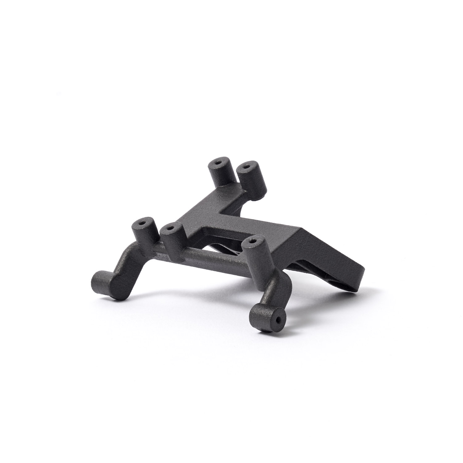
    Shapeways parts
    Shapeways parts

    The AI and Robotics Synergy

    The integration of AI into robotics is not just a trend; it’s a revolution. Companies are increasingly relying on Shapeways to meet the burgeoning demand for AI-powered robotic products. The reason? Shapeways’ Enterprise Manufacturing Solutions offering, which has been instrumental in acquiring new business from long-standing customer relationships.

    The numbers speak for themselves. With the robotics industry projected to be worth a whopping $260 billion by 2030, Shapeways is strategically positioning itself as a pivotal player. A testament to this is their recent expansion of a multi-year partnership with a leading robotics firm specializing in AI-driven robots for healthcare.

    Shapeways parts
    Shapeways parts

    Digital Manufacturing: The Game Changer

    Shapeways’ success doesn’t just stem from its ability to manufacture parts. It’s their innovative approach to digital manufacturing that’s making waves. As Aidan O’Sullivan, GM of Enterprise Solutions for Shapeways, rightly points out, the value of digital manufacturing for robotics is immense. It offers scalability, customization, and efficiency, minimizing overheads and maximizing output.

    But it’s not just about additive manufacturing. Shapeways’ expertise in tooling and molding, especially for high-volume parts, plays a pivotal role in their success story.

    The Broader Impact

    Shapeways’ impact isn’t limited to healthcare. They’ve also expanded their partnership with a top robotics manufacturer in the industrial supply chain, witnessing a fourfold increase in revenue year-over-year. This underscores the versatility and flexibility of digital manufacturing, especially when powered by AI and automation.

    According to Precedence Research, the global market valuation of AI in manufacturing is set to reach a staggering USD $68.4 billion by 2032. This projection underscores the transformative potential of AI in reshaping the manufacturing landscape.

    Looking Ahead

    As Greg Kress, CEO for Shapeways, emphasizes, the company’s dedication goes beyond mere manufacturing. They’re committed to fostering innovative advancements in the robotics sector. With AI’s increasing adoption, robotics is set to become even more integrated across various industries, automating processes and harnessing innovation.

    In conclusion, as robotics continues to evolve with AI capabilities, Shapeways is uniquely positioned to drive innovative solutions across sectors. For those keen on delving deeper into this fascinating intersection of AI, robotics, and manufacturing, keeping an eye on Shapeways’ journey might offer valuable insights.

    Source: Shapeways Holdings, Inc. Press Release

  • IperionX Achieves UL Validation for 100% Recycled Titanium: A Sustainable Breakthrough

    IperionX Achieves UL Validation for 100% Recycled Titanium: A Sustainable Breakthrough

    In a groundbreaking achievement, IperionX Limited, a pioneering force in titanium metal production, has achieved the highly coveted UL Environmental Claim Validation for its 100% recycled, low-carbon titanium metal powder. This validation marks a significant milestone in the additive manufacturing industry, positioning IperionX as the first company to attain UL recognition for its commercial titanium powder made entirely from recycled content.

    Reviving Titanium’s Sustainable Potential: The validation holds immense importance as titanium metal powder used in additive manufacturing can only be recycled a limited number of times before its quality is compromised by contaminants or inferior powder morphology. Such out-of-specification titanium powder poses a threat to the structural integrity of additively manufactured components. Furthermore, the conventional “Kroll Process” for titanium production is marred by high energy consumption, exorbitant costs, significant carbon emissions, and low levels of circularity. This conventional approach generates substantial volumes of titanium waste that often end up downcycled or landfilled.

    Enter IperionX’s Low-Carbon Solution: Contrasting the status quo, IperionX presents a revolutionary solution with its low-carbon titanium. With zero scope 1 and 2 emissions, IperionX utilizes 100% scrap titanium as feedstock, enabling the production of high-performance, low-carbon recycled titanium metal through a circular supply chain that eliminates reliance on mined resources. This approach not only reduces environmental impact but also offers manufacturers in diverse sectors, including automotive, defense, bicycle, consumer electronics, and green hydrogen, the opportunity to fulfill their sustainability targets.

    A Carbon Footprint Breakthrough: IperionX’s commitment to sustainability is further reinforced by the recently completed life cycle assessment (LCA) for its 100% recycled, low-carbon titanium metal. The assessment confirmed IperionX’s titanium as having the lowest quantified life cycle carbon footprint among commercial titanium powders. With a potential carbon footprint of only 7.8 kg of carbon dioxide equivalents (CO2e) per kg, IperionX’s forecasted footprint is over 90% lower than plasma-atomized titanium powders, 80% lower than Kroll process-produced titanium ingots, and more than 50% lower than aluminum ingots. Remarkably, it is on par with stainless steel ingots, showcasing IperionX’s unparalleled commitment to sustainability.

    Acknowledging Industry Recognition: IperionX’s exceptional achievements have not gone unnoticed. Recently, the company emerged victorious in the U.S. Air Force Research Laboratory Grand Challenge, where it outshone leading titanium companies by successfully producing high-quality titanium metal powder solely from titanium scrap feedstocks. This accolade further solidifies IperionX’s position as a trailblazer in the realm of low-carbon, recycled titanium production.

    Shaping the Future of Advanced Industries: As major industry players across space, aerospace, electric vehicles, and 3D printing embrace the need for low-carbon titanium sourced from traceable recycled origins, IperionX stands at the forefront of meeting their sustainability goals. The selection of materials plays a pivotal role in reducing carbon intensity without compromising durability, quality, or performance requirements. IperionX empowers these companies with a unique and invaluable solution that maximizes recycled content, lowers carbon footprints, and enables the production of high-performance titanium products.

    The UL validation for IperionX’s 100% recycled titanium powder marks a turning point in additive manufacturing’s sustainable journey. This achievement, combined with the results from their Life Cycle Assessment, reaffirms IperionX’s status as the market leader in low-carbon, 100% recycled titanium metal. With its groundbreaking technologies, operational pilot facility in Utah, and plans for a Titanium Demonstration Facility in Virginia, IperionX continues to drive the development of low-carbon titanium for advanced industries. By revolutionizing the manufacturing landscape, IperionX paves the way for a more sustainable future, one recycled titanium particle at a time.

  • NUBURU Introduces Next-Generation 1 Kilowatt Blue Laser Technology

    NUBURU Introduces Next-Generation 1 Kilowatt Blue Laser Technology

    NUBURU, a renowned leader in high-power and high-brightness industrial blue laser technology, has recently announced the introduction of its latest innovation, the NUBURU BL-1000-F. This next-generation 1-kilowatt blue laser is set to make a significant impact on several large and rapidly growing industries, including EV battery production, metal 3D printing, and consumer electronics. With its increased power and enhanced capabilities, the BL-1000-F is poised to revolutionize manufacturing processes and empower businesses to achieve new levels of efficiency and precision.

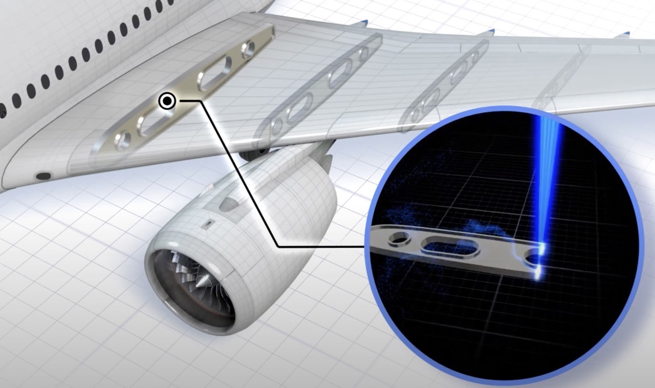
    Harnessing the Power of Blue Light: The NUBURU BL-1000-F stands out due to its ability to leverage the inherent high absorption of metals to blue light. This unique characteristic allows for superior performance in welding and processing applications. By utilizing the higher power delivered by the BL-1000-F, manufacturers can achieve higher quality laser beams, enabling efficient welding and processing of highly reflective metals that pose challenges for traditional infrared lasers. This breakthrough technology opens up new possibilities for EV battery production and metal additive 3D printing, where precision and process stability are crucial.

    Nuburu Blue Light Laser
    Blue Laser Area Printing – Nuburu

    Advancing Manufacturing Capabilities: The introduction of the BL-1000-F addresses the needs expressed by customers, who have eagerly awaited a solution that combines speed and weld quality. This powerful laser system enables higher speed and micron-level precision, paving the way for faster, more reliable, and repeatable high-quality welds. With the ability to meet these critical requirements, the BL-1000-F empowers manufacturers to enhance their capabilities across various industries.

    Enhanced Welding and Additive Manufacturing: One of the primary applications of the BL-1000-F lies in EV battery welding. As electric vehicles continue to gain momentum, the demand for efficient and reliable battery production methods increases. The BL-1000-F’s higher power and improved weld quality enable manufacturers to streamline their battery welding processes, ensuring optimal performance and longevity of these essential energy storage components.

    Additive Manufacturing wih Blue Laser - Nuburu
    Additive Manufacturing wih Blue Laser – Nuburu

    Additionally, the BL-1000-F’s impact extends to the metal additive 3D printing industry. With its ability to process reflective metals effectively, this blue laser technology opens up new avenues for printing intricate and high-quality metal parts. Manufacturers can achieve greater accuracy, faster printing speeds, and improved overall process stability, revolutionizing the way metal components are produced in various sectors.

    Unveiling at Laser World of Photonics: NUBURU will officially unveil the BL-500-F and the BL-1000-F at the prestigious Laser World of Photonics event in Munich on June 27, 2023. Visitors can explore these groundbreaking technologies firsthand at booth A2 103 (Laser 2000). This event marks a significant milestone in the advancement of blue laser technology and demonstrates NUBURU’s commitment to driving innovation in the manufacturing industry.

    With the introduction of the NUBURU BL-1000-F, the manufacturing landscape is set to undergo a transformative shift. This cutting-edge blue laser technology unlocks new possibilities for EV battery production, metal additive 3D printing, and consumer electronics manufacturing. The BL-1000-F’s higher power, speed, and precision will empower businesses to achieve greater efficiency, superior weld quality, and improved overall manufacturing capabilities. Stay tuned for more updates on NUBURU’s breakthrough solutions and their impact on the industry.

  • Additively Manufactured Electronics: Processes, Materials, Applications and Limits

    Additively Manufactured Electronics: Processes, Materials, Applications and Limits

    Additively manufactured electronics (AME) combines additive deposition of conductive, dielectric and structural materials to create electronic functions on, within or around three-dimensional parts. It overlaps with printed electronics, but AME places greater emphasis on multilayer, three-dimensional and embedded structures.

    AME does not automatically replace conventional printed circuit boards. Its strongest use cases are geometries, prototypes and integrated functions that planar PCB manufacturing handles poorly.

    AME, printed electronics and conventional PCBs

    ApproachTypical structureStrengthLimitation
    Conventional PCBPlanar rigid or flexible laminate with patterned copper and assembled componentsMature density, conductivity, reliability and supply chainLimited freedom for fully three-dimensional interconnect geometry
    Printed electronicsDeposited conductive or functional inks on flexible or rigid substratesLarge-area, low-temperature and flexible functionalityOften lower conductivity and feature density than copper PCB processes
    Additively manufactured electronicsMultilayer or 3D combination of dielectric and conductive materials, sometimes with embedded componentsConformal, volumetric and customized electronic structuresMaterials, resolution, component integration and qualification remain challenging
    In-mold electronicsPrinted functional layers and components integrated into a molded polymer partThin smart surfaces and part consolidationForming, molding, interconnection and lifecycle reliability

    Main AME process families

    Inkjet printing

    Inkjet systems eject controlled droplets of conductive, dielectric or functional ink. They can pattern fine features without a physical mask and support rapid design changes. Stable jetting requires tight control of viscosity, surface tension, particle size, nozzle condition and substrate wetting.

    Aerosol jet printing

    Aerosol jet printing atomizes an ink and focuses the aerosol stream through a nozzle. It can deposit fine traces on planar, curved or stepped surfaces and is used for antennas, sensors, interconnects and repair. Overspray, line-edge definition, adhesion and curing must be controlled.

    Direct ink writing and microdispensing

    Direct ink writing extrudes pastes or viscoelastic inks through a nozzle. It supports thicker conductors, dielectric structures, sensors and embedded features. Resolution is generally coarser than inkjet or aerosol jet, but deposited cross-section and material range can be larger.

    Multi-material 3D printing

    Some platforms alternate dielectric and conductive deposition to build multilayer electronic structures. Components may be placed into cavities during pauses and then connected or encapsulated. This requires registration between materials, controlled interface quality and a robust component-placement strategy.

    Laser-based and hybrid methods

    Laser direct structuring, laser-induced forward transfer, selective sintering and hybrid print-and-plate routes can create or improve conductive paths. These are often combined with conventional plating, component assembly, machining or molding rather than used as standalone processes.

    Materials used in AME

    Material classExamplesCritical properties
    Conductive inks and pastesSilver, copper, gold, carbon and conductive polymersConductivity, oxidation, viscosity, particle size, adhesion and cure temperature
    DielectricsPhotopolymers, epoxies, polyimides and ceramic-filled formulationsPermittivity, dielectric strength, loss, moisture uptake and thermal stability
    Structural substratesThermoplastics, thermosets, ceramics, glass and compositesSurface energy, coefficient of thermal expansion, stiffness and processing temperature
    Resistive and sensing materialsCarbon systems, metal oxides, piezoresistive inks and functional compositesSensitivity, drift, hysteresis, selectivity and environmental stability
    EncapsulantsPolymers and barrier coatingsMoisture protection, chemical resistance, adhesion and reworkability
    Component interconnect materialsConductive adhesives, solder and printed interconnectsContact resistance, fatigue, cure compatibility and repair

    Conductivity is a central limitation

    Printed metallic traces often have lower electrical conductivity than bulk or plated copper because of porosity, organic binders, incomplete sintering and small cross-section. Electrical performance depends on:

    • Ink composition and metal loading
    • Line width, thickness and continuity
    • Drying and sintering profile
    • Substrate temperature capability
    • Oxidation, especially for copper
    • Surface roughness and wetting
    • Bends, vias and material interfaces
    • Environmental aging and mechanical cycling

    A trace that conducts at room temperature after printing may still fail under current load, humidity, thermal cycling or flexing. Final resistance and power-handling capability should be measured in the finished geometry.

    Dielectric and RF performance

    For antennas, high-frequency interconnects and embedded RF structures, the dielectric material is as important as the conductor. Relevant variables include dielectric constant, loss tangent, thickness uniformity, moisture absorption and surface roughness.

    • Printed dimensions must match the electromagnetic design after cure and shrinkage.
    • Material properties should be measured at the operating frequency.
    • Conductor roughness and porosity can increase RF loss.
    • Transitions to connectors, chips or conventional boards often dominate performance.
    • Protective coatings can change antenna tuning and dielectric behavior.

    Component embedding

    AME systems can pause printing to place resistors, capacitors, sensors, chips or packaged components into a cavity. The process then prints connections or encapsulates the component. Key questions include:

    • Can the component tolerate deposition and curing temperatures?
    • How is placement accuracy maintained?
    • How are terminals cleaned and connected?
    • Does encapsulation create thermal stress or voids?
    • Can the component be inspected, reworked or replaced?
    • How is heat removed during operation?
    • What happens when the structural and electronic lifetimes differ?

    Applications where AME creates value

    Conformal antennas

    Conductive traces can be printed on curved housings, airframes, vehicle surfaces or compact devices. This can reduce separate antenna parts and enable geometry matched to the product. RF tuning, grounding, shielding and environmental durability remain critical.

    Sensors and smart structures

    Strain, temperature, pressure, chemical or capacitive sensors can be deposited on or embedded within a component. AME can shorten wiring and place sensing closer to the physical event, but calibration drift, cross-sensitivity and repair must be evaluated.

    Rapid electronic prototypes

    AME can reduce the time required to create low-volume test circuits, unusual interconnects, RF coupons or integrated demonstrators. This is particularly useful when a conventional PCB shape cannot represent the final product geometry.

    In-mold and structural electronics

    Printed conductors, touch controls, lighting and sensors can be formed and molded into automotive or consumer surfaces. IPC-8401, released in 2024, provides guidelines for in-mold electronics covering process structures, materials and production test methods.

    Biomedical and wearable devices

    Flexible sensors, electrodes and customized housings are promising uses. Skin contact, washability, motion, moisture and biological compatibility require application-specific controls. Implantable electronics involve a much higher evidence burden than external wearables.

    Where conventional PCB manufacturing remains stronger

    • Very high interconnect density
    • Fine multilayer vias and controlled impedance
    • High-current copper distribution
    • Established component assembly and reflow
    • High-volume low-cost production
    • Mature reliability standards and test infrastructure
    • Repairability and replaceable board architecture
    • Broad global supplier availability

    Many successful AME products will be hybrid: conventional chips and boards combined with printed antennas, sensors, interconnects or structural features.

    Reliability risks

    RiskPossible mechanismTypical evaluation
    Open circuitCracking, poor deposition, interface separation or oxidationContinuity monitoring and thermal/mechanical cycling
    Resistance driftMicrostructural change, moisture or conductor damageFour-point resistance and aging tests
    Short circuitOverspray, dielectric breakdown, migration or contaminationInsulation resistance and high-potential testing
    DelaminationThermal-expansion mismatch or weak surface preparationAdhesion, peel and environmental cycling
    RF performance shiftGeometry change, moisture, coating or conductor lossS-parameter and antenna-pattern measurement
    Component-joint failureCure stress, vibration, thermal fatigue or poor contactCross-section, electrical testing and life cycling
    Encapsulation failureVoid, cracking or moisture ingressMicroscopy, leak, humidity and thermal-shock testing

    Qualification and standards

    AME standards are less mature than conventional PCB standards. IPC’s standards program lists IPC-6911, “Acceptability of Additively Manufactured Electronics,” as an approved standards-development project. Printed-electronics standards already address flexible and rigid substrates, materials and terminology, while IPC-8401 covers in-mold electronics.

    1. Define application class, environment and electrical function.
    2. Specify conductor, dielectric, substrate and component materials.
    3. Validate geometry, registration, layer thickness and curing.
    4. Measure final electrical and RF properties.
    5. Test adhesion and interfaces after environmental exposure.
    6. Verify embedded-component placement and interconnects.
    7. Define inspection methods for hidden layers and features.
    8. Run thermal, humidity, vibration and mechanical life tests.
    9. Control software, inks, substrates and process changes.
    10. Retain a digital data package linking design to tested hardware.

    Production economics

    AME can avoid masks, tooling, separate wiring and assembly, but it can also introduce expensive inks, slow deposition, curing, component placement and inspection. The strongest economic cases usually involve:

    • Low-volume or frequently changing designs
    • Conformal or volumetric geometry
    • Part consolidation with measurable weight or assembly value
    • High-value sensing or RF functionality
    • Short prototype or development cycles
    • Hybrid manufacturing where AME replaces only the difficult portion

    Compare total cost—including inks, curing, failed deposition, component placement, test and yield—with a conventional PCB, flexible circuit, molded interconnect device or wired assembly.

    Application-selection checklist

    • The electronic function benefits from a 3D or conformal shape.
    • Required conductivity and current are within printed-material capability.
    • The substrate tolerates deposition and cure.
    • Component placement and thermal management are feasible.
    • Hidden conductors and interfaces can be inspected or process-controlled.
    • Environmental reliability can be demonstrated.
    • Repair and end-of-life strategy are acceptable.
    • The total system beats conventional or hybrid alternatives.

    Conclusion

    Additively manufactured electronics expands electronic design beyond planar boards by enabling conformal conductors, embedded sensors and volumetric structures. The technology is strongest when 3D integration creates real product value. Conventional PCBs remain superior for many dense, high-volume and high-reliability circuits, making hybrid architectures the most practical path for many applications.

    Related Addithive resources: Industrial AM Software Guide · Scaling AM Production · Nano Dimension AM Profile

    References and further reading

  • Fuji and J.A.M.E.S. Partner to Advance Additive Electronics

    Fuji and J.A.M.E.S. Partner to Advance Additive Electronics

    In an exciting development for the additive manufacturing industry, Fuji Corporation, a renowned Japanese technology company, has recently formed a strategic partnership with J.A.M.E.S. GmbH, a leading German firm specializing in Additively Manufactured Electronics (AME). This collaboration aims to propel the growth of additive electronics and revolutionize the way electronic devices are manufactured. The partnership brings together Fuji’s innovative electronics 3D printer, FPM-Trinity, and J.A.M.E.S.’s expertise in building an online community dedicated to advancing AME technology.

    IoT Board Printed with FPM-Trinity Source : Fuji

    Fuji’s FPM-Trinity: A Game-Changing Electronics 3D Printer

    At the heart of this partnership lies Fuji’s groundbreaking electronics 3D printer, the FPM-Trinity. This unique machine combines resin substrate printing, circuit printing, and component mounting capabilities, allowing for the complete additive manufacturing of electronic devices in a single process. The FPM-Trinity eliminates the need for multiple manufacturing steps, streamlining the production of electronic components and reducing time-to-market.

    J.A.M.E.S.: Pioneering AME and Enabling Collaboration

    J.A.M.E.S., an abbreviation for “Joint Additively Manufactured Electronics Standarization,” was established with a specific mission to promote the development of AME. The company has created an online community that serves as a hub for manufacturers and users to collaborate, communicate, and share knowledge in real time. By joining forces with Fuji, J.A.M.E.S. aims to explore the full potential of AME and make it a technology accessible to all.

    Advantages of the Partnership

    Through this partnership, Fuji intends to leverage J.A.M.E.S.’s network to exchange information and enhance the value of its products. The collaboration will provide Fuji with valuable insights from end-users, which can influence the company’s business strategy and future product development. Moreover, the partnership opens doors for Fuji to propose novel ideas and solutions using the FPM-Trinity, driving the adoption of AME across the electronics industry.

    IoT Board Printed with FPM-Trinity Source : Fuji

    FPM-Trinity’s Key Features and Benefits

    The FPM-Trinity offers a range of features that make it a game-changer in the world of additive electronics:

    1. All-in-One Solution: This electronics 3D printer combines resin printing, circuit printing, and parts placement within a single machine, streamlining the manufacturing process.
    2. Direct Digital Printing: FPM-Trinity enables direct printing from CAD data, eliminating the need for additional processes such as mask creation. This feature saves time and increases efficiency.
    3. Rapid Turnaround: With FPM-Trinity, it is possible to go from data input to completion within a single day, significantly reducing production timelines.
    4. 3D Form Factor: The FPM-Trinity allows the creation of electronic devices with complex 3D geometries, expanding design possibilities and enabling innovative product development.
    5. Sustainable Manufacturing: By minimizing waste materials and optimizing material usage, the FPM-Trinity contributes to sustainable manufacturing practices.

    Future Developments and Impact of AME

    Fuji Corporation currently offers a sample manufacturing service utilizing the FPM-Trinity. However, their long-term goal is to release the machine for sale, advancing the development and widespread adoption of additive manufacturing technology. This initiative is expected to address industry challenges such as the rapid growth of the Internet of Things (IoT), the pursuit of sustainability, and the need to shorten product development cycles.

    Understanding Additively Manufactured Electronics (AME)

    Conventionally, printed circuit boards (PCBs) are manufactured through subtractive processes, involving etching away unnecessary materials. In contrast, AME utilizes 3D printing techniques to selectively apply materials only where required, resulting in minimal material waste and liquid

  • Breaking the Barrier: EOS and nTopology Join Forces to Eliminate Additive Manufacturing Bottlenecks

    Breaking the Barrier: EOS and nTopology Join Forces to Eliminate Additive Manufacturing Bottlenecks

    In a groundbreaking collaboration, nTopology, the leading engineering design software developer, and EOS, the industrial 3D printing industry pioneer, have announced a significant breakthrough in additive manufacturing (AM) workflow. The development of a new Implicit Interop capability aims to solve a major bottleneck in the industry by enabling the transfer of highly complex designs in megabyte-sized files, thereby revolutionizing the time to manufacturing.

    Industrial heat exchanger printed on EOS M 290 Source: EOS

    Traditionally, file sizes for 3D printers could reach tens of gigabytes, posing significant challenges for the manufacturing process. However, nTopology and EOS have now introduced the nTop Implicit File, which can drastically reduce file sizes by up to 99%, generate files 500 times faster, and achieve 60% faster load times. These advancements make the technology more accessible to AM build preparation software, expediting the entire manufacturing workflow.

    One of the impressive demonstrations at the Formnext 2022 event in Frankfurt, Germany, featured a large industrial heat exchanger, designed by Siemens Energy as a proof-of-concept. The intricate design, exported to an nTop Implicit File within seconds, required less than 1 MB of storage space. The file was then seamlessly imported into EOSPRINT, where it was used to additively manufacture the heat exchanger using an EOS M 290 industrial 3D printer. This successful application showcased the immense potential of the Implicit Interop technology.

    To drive broader adoption of their innovation, nTopology and EOS are collaborating with the 3MF Consortium to standardize the Implicit File format. This collaboration aims to incorporate the technology into a future update of the 3MF industry-standard 3D printing file format, further enhancing compatibility and ease of use across the industry.

    Bradley Rothenberg, nTopology Co-founder and CEO, expressed the company’s commitment to empowering engineers with design freedom and enabling the production of complex parts. By working closely with EOS, they developed a solution to address the design data bottlenecks encountered in printing intricate designs. This partnership exemplifies their dedication to advancing the industry and fostering collaborations with original equipment manufacturers (OEMs).

    Industrial heat exchanger printed on EOS M 290 Source : EOS

    Alexander Bockstaller, Software Product Line Manager at EOS, acknowledged the rising complexity of part geometries due to modern design approaches like topology optimization, generative design, and design for additive manufacturing (DfAM). These advancements have necessitated a solution to handle large and intricate meshes more efficiently. EOS takes up the challenge by driving the standardization of implicit geometry representation, making it possible to build designs that were previously unattainable.

    Ole Geisen, Head of Engineering Services for Additive Manufacturing at Siemens Energy, applauded the technical development achieved by nTopology and EOS. He emphasized that the rest of the additive manufacturing ecosystem now needs to catch up with these advancements. As topology optimization, generative design, and DfAM continue to push the boundaries of complexity in part geometries, exchanging such intricate designs using traditional data formats becomes increasingly challenging. The Implicit Interop technology is a game-changer, removing a significant barrier and paving the way for innovation in thermal management and beyond.

    The introduction of the Implicit Interop capability by nTopology and EOS marks a pivotal moment in the additive manufacturing industry. This technological breakthrough not only addresses the long-standing bottleneck of handling large file sizes but also unlocks new possibilities for engineers and designers to create complex and innovative products. As the implicit geometry representation becomes standardized, the industry can expect improved interoperability, streamlined workflows, and accelerated adoption of advanced design techniques. With continued collaborations and advancements, the future of additive manufacturing looks promising and full of exciting opportunities.

  • Redwire Subsidiary Awarded Contract with European Space Agency to Revolutionize Tissue Manufacturing in Space and on Earth

    Redwire Subsidiary Awarded Contract with European Space Agency to Revolutionize Tissue Manufacturing in Space and on Earth

    In a groundbreaking development for the future of space exploration and biomedical research, Redwire Corporation, a prominent player in the space industry, has announced that its subsidiary, Redwire Space NV, has secured a 14 million euro contract from the European Space Agency (ESA). This exciting partnership aims to develop the 3D-BioSystem Facility, an advanced 3D bioprinting system that will enhance tissue manufacturing capabilities for long-duration space missions and have significant implications for life on Earth.

    A Giant Leap for Bioprinting:

    The 3D-BioSystem Facility, designed and developed by Redwire Space NV, will be a cutting-edge modular system that harnesses the power of 3D bioprinting technology. With its ability to sustain a multitude of experiments, this facility represents a significant leap forward in microgravity bioprinting capabilities. The system will consist of a 3D bioprinter, 3D cell culture units, and an incubator, enabling the production of tissue samples directly in space. These samples can then be further processed onboard or returned to Earth for further analysis and application.

    Paving the Way for Space Exploration:

    One of the primary goals of the 3D-BioSystem Facility is to enable long-duration spaceflight to destinations such as the Moon and Mars. The ability to bioprint cell constructs in microgravity is crucial for sustaining astronauts during these ambitious missions. By leveraging tissue engineering and regenerative medicine, the facility will contribute to the development of vital resources and medical treatments for space travelers. Moreover, the system could potentially revolutionize the way we understand cell-to-cell interactions, advance drug efficacy and toxicity testing through organoid creation, and pave the way for printing vascularized tissue and transplantable organ patches.

    International Space Station

    Advancing Biomedical Research on Earth:

    The impact of the 3D-BioSystem Facility extends far beyond the realm of space exploration. By enhancing our understanding of tissue engineering and bioprinting, the facility holds immense promise for improving healthcare and advancing medical research here on Earth. Through studying cell behavior in three-dimensional environments and investigating the effects of microgravity on tissue growth, scientists can gain crucial insights into complex diseases and develop innovative therapies. The facility’s potential applications range from personalized medicine to drug discovery, creating opportunities to address unmet medical needs and improve patient outcomes.

    Boosting European Technological Independence:

    The partnership between Redwire Space NV and the European Space Agency is also significant in terms of fostering European technological non-dependence and competitiveness. By developing state-of-the-art space infrastructure and leveraging advanced manufacturing techniques, Europe can secure its place as a leader in space innovation. This not only ensures the continent’s access to space benefits but also contributes to the expansion of the global space economy.

    International Space Station

    Redwire’s Track Record and On-Orbit Capabilities:

    Redwire Corporation has established itself as a frontrunner in microgravity bioprinting, exemplified by its BioFabrication Facility (BFF) currently operating on the International Space Station (ISS). The BFF-Meniscus-2 investigation, a collaboration between Redwire and the Uniformed Services University of the Health Sciences Center for Biotechnology, showcases the potential of space bioprinting to treat meniscal injuries. With the 3D-BioSystem Facility joining the ranks, Redwire’s on-orbit capabilities continue to advance biomedical research, plant biology, and advanced materials manufacturing, fostering scientific discovery and facilitating the development of beneficial products for Earth.

    The Redwire subsidiary’s contract with the European Space Agency marks a significant milestone in the field of additive manufacturing and space exploration. The 3D-BioSystem Facility’s development represents a

  • Additive Manufacturing Trends in 2023 — Historical Industry Snapshot

    Additive Manufacturing Trends in 2023 — Historical Industry Snapshot

    This article is an archive of 2023 expectations

    This page was originally published as a forward-looking list of additive manufacturing trends for 2023. It is now preserved as a historical snapshot rather than a current industry outlook.

    The original themes—powder bed fusion, automation, new materials, vat photopolymerization, directed energy deposition, binder jetting and production scaling—remain relevant process categories. However, the article used overly promotional language and did not distinguish between technical possibility, commercial adoption and qualified production.

    How to read the original 2023 themes today

    2023 themeMore durable interpretationCurrent Addithive resource
    Powder bed fusionA mature process family whose limits depend on material, machine, geometry and qualificationLPBF terminology guide
    AutomationA factory-flow and data problem, not simply robotic printer loadingScaling AM production
    Novel materialsUseful only when feedstock, process window, post-processing and design data mature togetherMetal AM process selection
    Vat polymerizationA broad family covering SLA, DLP, MSLA and continuous-interface approachesVat photopolymerization guide
    Directed energy depositionA family whose economics depend on deposition, machining and inspection as one routeWAAM guide
    Binder jettingPrinting speed must be evaluated together with depowdering, debinding and sinteringBinder jetting guide
    High-volume productionAccepted-part throughput depends on yield and downstream bottlenecksProduction scaling

    Subscribe to continue reading

    Subscribe to get access to the rest of this post and other subscriber-only content.