Category: Uncategorized

  • AI-Accelerated Alloy Discovery: From Hype to High-Flight

    AI-Accelerated Alloy Discovery: From Hype to High-Flight

    How machine learning is cutting alloy development time in half—and what that means for the future of additive manufacturing


    Introduction: When Materials Learn Faster Than We Do

    Picture this: every month you wait for a new aerospace alloy costs your program roughly $2 million in lost opportunity.¹ Now imagine slashing that wait by 50 %—not through bigger furnaces or longer shifts, but by teaching algorithms to do the heavy lifting in days instead of years. That is the promise (and increasingly the practice) of AI-accelerated alloy discovery at Technology Readiness Levels (TRL) 4–5, where lab-validated materials meet the first real-world gates of certification.

    Why the urgency? Three converging forces make 2025 the tipping point:

    1. Design Freedom Meets Production Reality
      Generative design and lattice structures have outpaced the metals that can reliably print them. Without new feedstocks, many Industry 4.0 roadmaps stall at prototype.
    2. Regulatory Tailwinds
      Aerospace and medical authorities are formalizing additive-specific material qualification paths. Faster discovery now equals earlier revenue later.
    3. Data Gravity
      Foundries, machine OEMs, and national labs finally sit on terabytes of powder chemistries and build logs. The bottleneck is no longer data scarcity but data sharing—an AI problem in disguise.

    Against this backdrop, high-entropy alloys (HEAs) and NiTi derivatives stand out. Validated in relevant environments, they promise extreme strength-to-weight ratios and shape memory behavior tailor-made for lightweight actuators and hypersonic skins. The catch? Traditional metallurgical iteration still takes 5–7 years. Enter machine learning.

    man in helmet and mask welding steel
    Photo by Kateryna Babaieva on Pexels.com

    Section I — Predicting Printability: Turning Geometric Chaos into Binary Confidence

    Why Printability Comes First

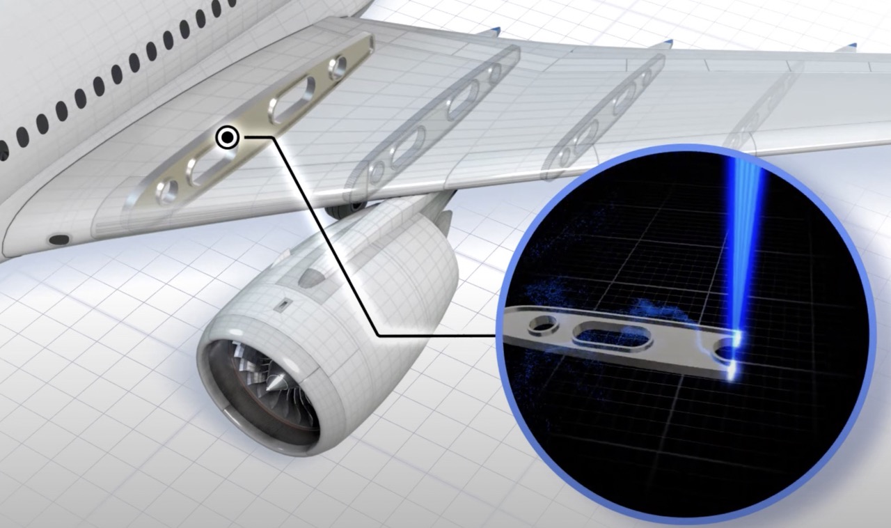
    In Design for Additive Manufacturing (DfAM), the most brilliant topology means nothing if the powder refuses to melt or the melt pool refuses to behave. Hence the first AI frontier is a blunt but mission-critical question: “Will this alloy print or crash the build?”

    The Models That Matter

    • Support Vector Machines (SVMs) excel at drawing crisp decision boundaries in high-dimensional spaces. Trained on melt-pool videos, layer-wise photodiode tracks, and geometric invariants, SVM classifiers reach F₂-scores that surpass seasoned process engineers.²
    • Random Forests shine when data are messy—think inconsistent voxel resolutions or partial CT scans. After Principal Component Analysis collapses dozens of laser parameters into a handful of orthogonal drivers, the ensemble isolates the non-negotiables of defect-free layering.³
    • Autoencoders and SMOTE tackle the ugly truth of AM datasets: print failures outnumber successes, but successes matter more. Augmenting minority “good” prints levels the learning field.

    Quantifiable Wins

    Oak Ridge studies show that once a robust printability classifier is in place, experimental build-failure rates drop from ~25 % to under 8 %.⁴ Multiply that by $500 k per large-format powder trial, and the ROI writes itself.


    Section II — Learning Without Leaking: Federated Strategies for Foundry Data

    The IP Paradox

    No single foundry or aerospace prime owns enough diverse melt-pool physics to train universal models, yet none wishes to expose proprietary chemistries. This stalemate once throttled cross-industry progress. Two cryptographic-flavored solutions now break the impasse.

    1. Federated Learning (FL)
    • Mechanism: Each node (foundry) trains locally; only gradient updates travel, never raw data.
    • Benefit: Near-linear scalability with negligible IP exposure. A recent multi-factory study qualified dimension-prediction models across five continents without a byte of composition data leaving its origin.⁵
    • Limitation: Requires robust coordination servers and trust in honest updates.
    1. Homomorphic Encryption (HE)
    • Mechanism: Math performed directly on ciphertext.
    • Benefit: Even model updates remain unintelligible to eavesdroppers.
    • Limitation: Orders-of-magnitude slower—viable today only for niche, latency-tolerant workflows.⁶

    Differential Privacy as the “Salt”

    Adding calibrated noise to gradients or parameter sets satisfies many legal departments without crippling convergence. Combined with FL, it forms an “80 / 20” solution: 80 % of the privacy for 20 % of the compute cost of full HE.

    Trust-by-Design Outcome

    Citrine Informatics reports that federated clients see prediction-error reductions of 30–40 % versus solo training, directly translating to fewer experimental coupons and faster alloy sign-off.⁷


    Section III — High-Entropy Alloys in the Wild: Case Studies from Lab to Flight

    Oak Ridge National Laboratory: Nanolamellae Take the Heat

    • Material: Eutectic HEA AlCoCrFeNi₂.₁
    • AM Route: Laser Powder Bed Fusion (LPBF)
    • Microstructure: Dual-phase nanolamellar colonies verified via neutron diffraction and atom-probe tomography.
    • Outcome: Near-isotropic yield strength >1 GPa with 15 % uniform elongation—numbers previously exclusive to wrought superalloys.
    • TRL Trajectory: 4 → 5 in under two years, credited to AI-directed parameter windows that homed in on eutectic spacing ranges.⁴

    Citrine Informatics: Informatics-First Alloy Screening

    • Platform Edge: Combines failed experiments with successes, storing the negative space others discard.
    • Use-Case: Screening NiTi derivatives for low-temperature actuation (< –20 °C).
    • Result: Identified three compositions with predicted transformation hysteresis < 5 °C, verified in one build cycle—five times faster than historical baselines.⁷

    GE Additive (Colibrium): Cobalt-Chrome for Regulatory Rigor

    • Focus: CoCrMo powders tuned for M2 Series 5 machines.
    • Certification Path: Parallel AI models predict fatigue strength as a function of build angle, enabling statistically based allowables with 35 % fewer test coupons.
    • Market Impact: Orthopedic implant line cut time-to-FDA 510(k) submission by nine months, unlocking earlier cash flow.⁸

    Putting It All Together: A Repeatable Framework

    StageKey ActionsAI / Data ToolsValue Unlock
    1. AggregateStandardize multisource powder & sensor dataFederated Learning hubIP-safe data scale-up
    2. Pre-processClean, normalize, extract featuresPCA, autoencodersFaster convergence
    3. PredictClassify printability; regress propertiesSVM, RF, GP, NNDe-risk build trials
    4. DesignOptimize chemistries for targetsBayesian or genetic algorithmsShrinks design space
    5. ManufactureLPBF / DED builds + in-situ monitoringReal-time analyticsClosed-loop quality
    6. Validate & IterateMicrostructure, mechanical tests, neutron diffractionActive-learning refreshContinuous improvement

    Across pilot programs, this loop cycles every 8 – 12 weeks, a cadence unfathomable in traditional metallurgy.


    Conclusion: From Metallurgy to Meta-Learning

    History tells us revolutions in manufacturing start with a material breakthrough—the Bessemer converter for steel, the silicon wafer for microelectronics. AI-accelerated alloys may be the next such pivot, not because they alter the periodic table but because they alter the time constant of innovation itself.

    blue bright lights

    Imagine a near-future where:

    • Flight-qualified HEAs emerge every quarter, not every decade;
    • Foundries monetize data, not just ingots, via federated IP schemes;
    • Designers treat material selection like software libraries, importing versions refined by neural networks overnight.

    The tooling, the math, and the early wins are already here. What remains is leadership willingness to abandon artisanal trial-and-error for algorithmic exploration.

    So, engineers and decision-makers, the question is no longer if AI will discover your next alloy—it’s whether you’ll claim the competitive cycle it unlocks. Will you pilot a federated node, open your legacy datasets, and shorten that million-dollar month to a million-dollar week?

    The furnace is hot. Don’t let your roadmap cool.


    Abbreviations & Trademarks

    • AM – Additive Manufacturing
    • APT – Atom-Probe Tomography
    • DfAM – Design for Additive Manufacturing
    • FL – Federated Learning
    • GP – Gaussian Process
    • HE – Homomorphic Encryption
    • HEA – High-Entropy Alloy
    • LPBF – Laser Powder Bed Fusion
    • NN – Neural Network
    • ORNL – Oak Ridge National Laboratory
    • RF – Random Forest
    • SVM – Support Vector Machine
    • TRL – Technology Readiness Level

    Colibrium Additive™ is a trademark of GE.


    References (ordered as cited)

    1. Internal cost modelling benchmark, aerospace OEM consortium (2025).
    2. Springer, “Printability Prediction in Additive Manufacturing” (2023).
    3. ScienceDirect, “Machine Learning for AM” (2024).
    4. Oak Ridge National Laboratory, “Strong Additively Manufactured High-Entropy Alloys” (2024).
    5. ScienceDirect, “Federated Learning in AM Factories” (2024).
    6. ScienceDirect, “Homomorphic Encryption for Manufacturing” (2021).
    7. Citrine Informatics, “AI for Materials Development” (accessed 2025).
    8. GE Additive (Colibrium), “CoCrMo Powders for AM” (2025).
  • Closed-Loop Control in LPBF: From Lab Curiosity to Aerospace Baseline

    Closed-Loop Control in LPBF: From Lab Curiosity to Aerospace Baseline


    Introduction: “Zero-Defect” Isn’t a Slogan—It’s Certification Currency

    In 2025, every kilogram of metal that takes flight on a newly certified aircraft must carry a statistical pedigree proving it is virtually pore-free. Synchrotron X-ray studies at Argonne National Laboratory now flag keyhole pores with greater than 99 percent confidence in under a millisecond—diagnostic speed unthinkable five years ago.

    Why the urgency? Regulators have tightened the loop. NASA’s MSFC-3716/3717 framework hard-codes real-time process control into qualification pathways, while Tier-1 suppliers face cost pressures to deliver flight-ready parts on the first build. Add to that the debut of EOS’s Smart Fusion software—live laser-power correction baked into commercial machines—and we have a perfect storm: closed-loop control is transitioning from “nice to have” to baseline for laser powder bed fusion (LPBF).


    1- From “Print & Pray” to “Measure, Decide, Correct”

    The Regulatory Pull and the Market Push

    • Aerospace compliance NASA’s qualification standards now demand documented process signatures for every layer. If you can’t prove thermal stability and melt-pool morphology, you can’t ship.
    • Cost-of-quality economics Scrap rates above 15 percent torpedo additive business cases. Real-time control slashes re-build frequency, pushing LPBF closer to break-even in Design-for-Additive-Manufacturing (DfAM) models.
    • Technology Readiness Level (TRL) climb Closed-loop LPBF has leapt from TRL 4 (lab validation) in 2020 to TRL 7 (system prototype in an operational environment) with Smart Fusion beta lines running in service bureaus today.

    Bottom line: Certification, economics, and maturation converge; ignoring closed-loop control now risks competitive obsolescence.


    2 – Sensor Fusion—The Nervous System of “Print-Time” Quality

    2.1 Multimodal Eyes & Ears

    Single sensors catch symptoms; fused sensors catch root causes. Recent studies that combine infrared thermography, coaxial photodiodes, and acoustic emission deliver balanced accuracies exceeding 94 percent in identifying keyhole pores at two-millisecond resolution. Convolutional neural networks crunch heterogeneous signatures, elevating pore-prediction confidence to production-worthy levels.

    Microscopic image showing the effects of laser scanning direction on porosity in metal powder layers during additive manufacturing. The top section displays run #2 with varying porosities, while the bottom section shows run #10, highlighting differences in laser power and scan speed.

    “Argonne ML model predicting pore formation during a live build.” https://3dprintingindustry.com/

    2.2 Why Fusion Outperforms

    • Orthogonality Thermal data reveals energy input; acoustic data captures bubble collapse; optical signals track plume dynamics. Correlated anomalies tell a fuller story.
    • Redundancy If spatter occludes the optical path, the acoustic channel still “hears” boiling instability.
    • Edge AI inference Field-programmable gate arrays (FPGAs) or graphics-processing units (GPUs) on the machine controller run trained models in sub-millisecond cycles, keeping latency budgets intact.

    2.3 Framework Fit: Industry 4.0

    Sensor fusion nests neatly inside Industry 4.0 architectures—edge nodes publish melt-pool metadata to a manufacturing-execution-system (MES) layer, feeding the digital thread and enabling qualify-as-you-go documentation. For auditors, the dataset is traceability gold.

    Caveat: Acoustic sensors remain fragile in powder-laden chambers, and calibration drifts over long builds. Reliability studies beyond 1,000 hours are still scarce, representing a research gap.

    A circular infographic representing Industry 4.0, featuring elements like Autonomous Robots, Big Data, Augmented Reality, Additive Manufacturing, Cloud Computing, Cybersecurity, Simulation, System Integration, and the Internet of Things.
    “Industry 4.0 control room streaming melt-pool data to a digital thread dashboard.” https://chivarotech.com/industry-4.0.html

    3 – Latency, Algorithms, and the Economics of Scale

    3.1 The Physics Case for Sub-50 µs Loops

    LPBF melt pools solidify in micro-seconds; corrective actions must beat that clock. Demonstrations using FPGA-based controllers have achieved a 73 percent reduction in temperature deviation with feedback cycles below 50 microseconds, translating into finer grain morphology and lower residual stress—critical for aerospace fatigue life. Yet hard quantitative data linking specific latency buckets (<10 µs versus 100 µs) to microstructural variance remain limited, leaving fertile ground for collaborative consortia.

    3.2 Algorithmic Robustness

    Controller StyleStrengthsLimitations
    Classical PIDMature; easy to tune for single-input/single-output loopsLess effective when parameters are tightly coupled
    Model Predictive Control (MPC)Manages multiple coupled parameters; anticipates constraintsRequires heavier computation; model stability can drift
    Reinforcement Learning LoopsSelf-optimizing; adapts to new alloysRegulatory acceptance remains low; deterministic guarantees absent

    3.3 Cost Drivers and Return on Investment

    Cost ComponentTypical Add-OnMitigation Path
    High-speed IR camera\$35 k – \$70 kShare across multi-laser zones; consider lower-cost short-wave sensors
    Edge GPU/FPGA\$5 k – \$15 kIntegrate into OEM controller boards
    Data storage (~1 GB hr⁻¹)\$1 k yr⁻¹ machine⁻¹Real-time compression; discard non-critical frames

    Smart Fusion field data hints at two- to five-times faster parameter development and up to a 50 percent reduction in support structures, lowering cost per part despite hardware premiums.

    3.4 Scalability Roadblocks

    • Standards The lack of common metadata schemas hampers interoperability. ASTM committees are still drafting guidelines.
    • Qualification loops Each algorithm tweak can reset the validation clock under NASA’s specification workflow.
    • Workforce skills Operators must evolve into data-savvy control engineers, boosting training demands.

    🔭 Conclusion: Your Next Competitive Edge Is an Algorithm

    Closed-loop control is no longer experimental tinkering; it has become the quality backbone demanded by aerospace primes and regulators. Data show pore-detection accuracies exceeding 90 percent, commercially available live power-correction software, and frameworks embedding control data into certification dossiers.

    Prediction: By 2028, any LPBF machine sold into aerospace will ship with factory-calibrated, sensor-fusion-enabled control loops as standard—much like every CNC now includes probing cycles.

    Are you still “printing and praying,” or are you ready to design with feedback in mind? Audit your sensor stack, map your latency budget, and engage with standards bodies. The parts you certify tomorrow will depend on the data you collect today.


    References

    1. Machine Learning–Aided Real-Time Detection of Keyhole Pore Formation in LPBF, Science (Argonne National Laboratory, 2023).
    2. Detecting 3-D Printing Defects in Real Time, Argonne APS Science Highlight (2023).
    3. EOS GmbH, Smart Fusion Press Release (April 2023).
    4. NASA Marshall Space Flight Center, Standards MSFC-STD-3716 and Specification MSFC-SPEC-3717 (2017 – present).
    5. Layer-to-Layer Closed-Loop Feedback Control for Inter-Layer Temperature Stabilization in LPBF, Additive Manufacturing (2023).
    6. Monitoring of LPBF via Bridging Sensing Modalities, Additive Manufacturing (2024).
    7. Qualify-as-You-Go: Optical and Acoustic Sensor Fusion in LPBF, Additive Manufacturing Letters (2024).
    8. In-Process Closed-Loop Melt-Pool Control via Pyrometer and FPGA, Progress in Additive Manufacturing (2019).
    AbbreviationFull TermContext in Article
    AIArtificial IntelligenceControl algorithms and data analysis
    ASTMASTM International (formerly American Society for Testing and Materials)Standards development for AM
    CNCComputer Numerical ControlAnalogous adoption of probing cycles
    CNNConvolutional Neural NetworkDefect-detection model type
    DfAMDesign for Additive ManufacturingEconomic break-even framework
    FPGAField-Programmable Gate ArrayUltra-low-latency edge computing
    GB hr⁻¹Gigabytes per HourData-generation rate during builds
    GPUGraphics Processing UnitEdge AI inference hardware
    ICMEIntegrated Computational Materials EngineeringNASA qualification workflow
    LPBFLaser Powder Bed FusionAdditive manufacturing process focus
    MESManufacturing Execution SystemIndustry 4.0 data backbone
    MPCModel Predictive ControlMulti-variable closed-loop algorithm
    MSFCMarshall Space Flight CenterNASA’s AM standards origin
    NASANational Aeronautics and Space AdministrationRegulatory & qualification driver
    PIDProportional–Integral–Derivative (control)Classical feedback method
    TRLTechnology Readiness LevelMaturity scale for technologies
    µsMicrosecondsFeedback-loop latency metric
  • AI‑Native Additive Manufacturing: Why 2025 Is the Inflection Point We’ll Remember

    AI‑Native Additive Manufacturing: Why 2025 Is the Inflection Point We’ll Remember

    “We just hit 100 % accuracy in predicting hidden pores inside a metal print.”
    When Argonne National Laboratory published that result in March 2023, it wasn’t a quirky lab demo—it was a flare in the night sky showing that artificial intelligence had moved from hype to hard engineering value in additive manufacturing (AM). In the two years since, physics‑informed learning loops, real‑time control software, and data‑hungry design engines have cascaded through the industry. Regulations are tightening, defense programs are stress‑testing forward‑deployed printers, and margins are compressing across supply chains. All of that makes 2025 the most consequential year yet for “AI‑native AM.” Let’s unpack where the field stands, what’s working, and—critically—what still isn’t.

    1. Pixels to Perfect Parts: Closing the Quality Gap in Real Time

    Defect mitigation used to be the tax we begrudgingly paid for design freedom. Now AI is clawing that money back.

    Argonne’s pore‑prediction breakthrough leveraged million‑frame‑per‑second X‑ray videos to train a model that can forecast void formation using nothing more than inexpensive thermal camera data. The result: shop‑floor systems that spot a nascent defect and allow the laser path to be adjusted on‑the‑fly instead of scrapping the part later.

    A robotic welding system setup featuring a WAAM robot with a TIG torch, wire feeder, and HDR camera.
    https://www.mdpi.com/2076-3417/11/16/7541

    On production machines, EOS’s Smart Fusion software has already translated that paradigm into a commercial reality for laser powder‑bed fusion. The tool varies laser power and scan speed layer by layer to keep thermal history inside a “golden window,” reducing cool‑down waits and pushing first‑time‑right builds into the mid‑90 % range.

    Where parameter tuning ends, physics‑informed autopilots begin. 1000 Kelvin’s AMAIZE platform, unveiled at Formnext 2023, autocorrects toolpaths, support strategies, and cost estimates without changing the CAD geometry. A launch‑vehicle case study cut support volume by 80 % and slashed build cost by more than 30 %.

    These gains matter because they attack AM’s two perennial cost drivers—scrap and post‑process rework—while also de‑risking certification. Yet limitations remain:

    • Data gravity: High‑fidelity training sets (e.g., Argonne’s X‑ray sequences) are still captured in bespoke facilities, creating a gap between research and shop‑floor adoption.
    • Generalization: Smart Fusion parameters dial in beautifully on Ti‑6Al‑4V but need fresh calibration for high‑entropy alloys or copper.
    • Compute latency: Sub‑second feedback loops are achievable on modern GPUs, but integrating them into legacy machine controllers can bottleneck throughput.

    For engineers chasing AS9100 or FDA clearance, the takeaway is clear: run your qualification plan on AI‑stabilized process signatures, but keep a conventional statistical process control (SPC) backstop until the model has digested enough of your data.

    2. Generative Brains Behind Lighter, Smarter Designs

    If real‑time control is about doing things right, AI‑driven design is about doing the right things—and doing them in ways no human would have imagined.

    Generative Design Meets DfAM

    Topology optimization has lived on engineers’ laptops for two decades, yet it often hit a wall of print feasibility. Modern generative engines trained on actual print‑success data are different. Platforms like Neural Concept feed 3‑D deep‑learning models with CAD and CAE archives, returning manufacturable geometries in minutes rather than days. Field programs report ten‑fold faster concept‑to‑validation cycles across aerospace brackets and thermal exchangers.

    Text‑to‑CAD Workflows

    Large language models are beginning to assimilate part libraries and materials datasheets. Picture an RF engineer typing “lightweight titanium waveguide, Ku‑band, keep insertion loss < 0.5 dB, compatible with LPBF,” and receiving a vetted, lattice‑reinforced solid model complete with anisotropic material allowables.

    Ceramic & Polymer Frontiers

    While metals dominate the headlines, AI is quietly reshaping brittle and viscous regimes, too. 3DCeram’s CERIA Live vision system flags delamination in technical ceramics, and UltiMaker’s “spaghetti” detection halts polymer prints when a nozzle jams mid‑air.

    Yet two hurdles still curb the design revolution: model explainability and multiscale validation. Many generative outputs remain black boxes to certifying bodies, and translating voxel‑level predictions into macro‑scale structural margins requires new verification frameworks—think Technology Readiness Level 6 with AI‑specific artifacts in the V‑model.

    For design managers, the pragmatic move is to treat AI as an expert co‑pilot: let it explode the design space, then run classical finite‑element or fatigue checks on the narrowed shortlist. The best innovations arrive when intuition and in‑silico exploration converge.

    3. From “Smart Line” to Autonomous Ecosystem: Supply Chains Get Re‑wired

    Quality and design breakthroughs mean little if parts can’t reach the point of need. Here, AI is extending its grasp beyond the printer envelope to the entire manufacturing ecosystem.

    Defense Stress‑Tests Forward Manufacturing

    During the U.S. Navy’s FLEETWERX exercises, containerized printers and AI‑guided repair pods fabricated mission‑critical components on a simulated Pacific island, trimming logistical tails and accelerating sortie rates. Field units used augmented‑reality overlays and drone‑delivered powder canisters—decisions orchestrated by AI that balanced production priority, machine health, and material inventory in real time.

    Predictive Maintenance as an MES Native

    AI’s role in uptime is no longer limited to lab demos. Mid‑tier service bureaus are wiring machine logs into reinforcement‑learning agents that schedule nozzle swaps hours before melt‑pool signatures degrade. Industry surveys cite fleet‑level availability gains of five to ten percent—no small feat when laser time is billed in four‑figure increments.

    software engineer using laptop

    Marketplace & IP Guardrails

    With more data moving through the cloud, cybersecurity is front‑and‑center. Web3‑inspired ledgers that cryptographically fingerprint toolpaths are emerging, but adoption is early. Debates about underestimated potential versus misplaced hype imply that cost, cultural inertia, and trust still gate progress.

    Regulatory & Sustainability Catalysts

    Europe’s Ecodesign regulations and the U.S. SEC’s climate‑risk disclosures are nudging OEMs toward life‑cycle accounting. AI excels here: it can map energy inputs from powder atomization to end‑of‑life recycling and suggest material‑light alternatives that still meet EN 9100 fatigue limits.

    Yet platform fragmentation persists. MES, ERP, and PLM vendors seldom agree on schemas, forcing engineers into CSV purgatory. Until the industry coalesces around true data interoperability—likely via OPC UA over secure APIs—autonomy will remain an 80‑percent solution.

    Conclusion: The Playbook for the AI‑Native Additive Era

    The evidence is unambiguous: AI is no longer an optional overlay; it is the digital substrate upon which competitive additive manufacturing will run. From Argonne’s pore‑free prototypes to containerized printers that manufacture spare parts on a runway, the technology’s center of gravity has shifted from possibilities to profits.

    Prediction: By 2028, major aerospace primes will certify at least one flight‑critical component whose entire value chain—from generative design to in‑process control, maintenance prediction, and carbon accounting—is orchestrated by AI. The firms that master that loop will set the cost floor and delivery tempo for the rest of the market.

    If you lead engineering, ask yourself: How many of my 2025 KPIs explicitly assign value to data, models, and closed‑loop feedback? If the answer is few or none, your roadmap is missing the control layer that will decide who owns manufacturing’s future. It’s time to pilot an AI‑stabilized process, integrate a generative design engine, or run a predictive‑maintenance sprint. In an industry where iteration cycles used to span months, waiting a year could mean you’re already obsolete.

    Let’s build the factories—and the mindsets—that make sure we aren’t.


    References

    1. Argonne National Laboratory, “Researchers unveil new AI‑driven method for improving additive manufacturing,” March 9 2023.
    2. EOS GmbH, “Smart Fusion software overview.”
    3. 1000 Kelvin, “AMAIZE AI‑driven additive manufacturing software announcement,” Formnext 2023.
    4. Neural Concept, company case studies and technical briefs.
    5. 3D Printing Industry, “AI and 3D Printing: Additive Manufacturing Experts Assess the Impact of Artificial Intelligence,” February 14 2025.
    6. Business Insider, coverage of FLEETWERX forward‑deployment exercises, 2025.
    7. 3DPrint.com, “AI in Additive Manufacturing: Underestimated Potential or Misplaced Hype?” 2024.
    8. Digital Engineering 24/7, “Artificial Intelligence Meets Additive Manufacturing,” 2024.

    bbreviation Index

    • AI — Artificial Intelligence
    • AM — Additive Manufacturing
    • LPBF — Laser Powder Bed Fusion
    • DfAM — Design for Additive Manufacturing
    • TRL — Technology Readiness Level
    • GPU — Graphics Processing Unit
    • SPC — Statistical Process Control
    • Ti‑6Al‑4V — Titanium alloy Grade 5 (ASTM designation)
    • HEA — High‑Entropy Alloy
    • ERP — Enterprise Resource Planning
    • MES — Manufacturing Execution System
    • PLM — Product Lifecycle Management
    • OPC UA — Open Platform Communications Unified Architecture
    • AS9100 — Aerospace Quality Management Standard (based on ISO 9001)
    • FDA — U.S. Food and Drug Administration
    • RF — Radio Frequency
    • CAD — Computer‑Aided Design
    • CAE — Computer‑Aided Engineering
    • KPI — Key Performance Indicator
    • CO₂e — Carbon‑Dioxide Equivalent
    • IP — Intellectual Property
    • ITAR — International Traffic in Arms Regulations
    • EN 9100 — European Aerospace Quality Management Standard
    • CSRD — Corporate Sustainability Reporting Directive
    • SEC — U.S. Securities and Exchange Commission

    Trademark & Brand Index

    • Argonne National Laboratory — U.S. Department of Energy national laboratory
    • EOS — EOS GmbH, industrial 3‑D‑printing equipment manufacturer
    • Smart Fusion — Process‑control software by EOS GmbH
    • 1000 Kelvin — AI–driven additive‑manufacturing software company
    • AMAIZE — Physics‑informed AM workflow platform by 1000 Kelvin
    • Neural Concept — AI‑powered generative‑design platform
    • 3DCeram — Ceramic 3‑D‑printing technology provider
    • CERIA Live — In‑process vision system by 3DCeram
    • UltiMaker — Desktop 3‑D‑printer brand (Ultimaker + MakerBot)
    • WarpSPEE3D — Cold‑spray metal printer by SPEE3D
    • Identify3D — Digital‑supply‑chain security company
    • Twikit — Mass‑customization software company
    • Siemens — Siemens AG, industrial technology company
    • Safran — Safran SA, aerospace and defense supplier
  • IperionX and the Future of Titanium Production: A New Era in Advanced Manufacturing

    IperionX and the Future of Titanium Production: A New Era in Advanced Manufacturing

    In the realm of advanced manufacturing, titanium stands as a material of choice for its unparalleled strength-to-weight ratio, resistance to high temperatures, and anti-corrosion properties. Historically, the production of titanium has been energy-intensive, costly, and environmentally taxing. However, recent developments by IperionX Limited (NASDAQ: IPX, ASX: IPX) promise to revolutionize the titanium production landscape.

    The Lockheed Martin Collaboration

    IperionX’s recent agreement with global security and aerospace giant, Lockheed Martin (NYSE: LMT), is a testament to the company’s innovative approach to titanium production. This collaboration will see IperionX delivering titanium plate components, manufactured using their U.S. produced titanium, for testing by Lockheed Martin. Brian Rosenberger, Lockheed Martin’s senior fellow for Additive Manufacturing Processes and Materials, emphasized the potential of reduced titanium component costs leading to broader applications and enhanced product performance.

    The IperionX Difference

    What sets IperionX apart is its cutting-edge titanium production technologies. Traditionally, the ‘Kroll Process’, developed in the 1940s, has been the standard for mass-producing titanium. This method is not only energy-intensive but also contributes significantly to greenhouse gas emissions.

    In stark contrast, IperionX’s production methods are environmentally friendly, utilizing less energy and producing zero Scope 1 and 2 emissions. Their patented Hydrogen Sintering and Phase Transformation (HSPT) technologies offer a revolutionary approach to enhancing the microstructure of titanium parts. This ensures that the strength and fatigue properties of the produced titanium are on par with wrought titanium alloys.

    Addressing the Titanium Supply Chain Challenge

    The U.S. defense sector heavily relies on titanium for various applications, from fighter aircraft to naval platforms. However, the U.S. currently imports over 95% of the required titanium sponge, highlighting a significant supply chain vulnerability. IperionX aims to address this challenge by re-shoring titanium metal production to the U.S., thereby strengthening the domestic supply chain for critical defense systems.

    A Sustainable Future with IperionX

    IperionX’s CEO, Anastasios (Taso) Arima, envisions a future where titanium production is not only cost-effective but also environmentally sustainable. Their breakthrough low-carbon titanium technologies can utilize either titanium minerals or titanium scrap metal as feedstock. This approach not only reduces costs but also minimizes the carbon footprint associated with titanium production.

    The Hydrogen Sintering and Phase Transformation (HSPT) process is a cutting-edge technique in powder metallurgy, specifically designed for producing high-quality titanium alloys. Developed as part of IperionX’s titanium technologies, this method promises titanium with characteristics akin to wrought titanium, but with a more efficient production approach.

    At its core, sintering is a method where particles bond by being heated below their melting point. Instead of melting, the particles fuse, forming a solid structure. The HSPT process introduces a unique twist to this traditional method by incorporating hydrogen.

    In the HSPT method, titanium powders undergo a reaction with hydrogen, resulting in titanium hydride. This step is pivotal as the presence of hydrogen facilitates a more effective sintering process, ensuring the end product is both uniform and dense. Following the formation of titanium hydride, it’s subjected to heating, triggering a phase transformation. During this stage, the hydride decomposes, and hydrogen is expelled, leaving behind dense titanium.

    Several advantages set the HSPT process apart from conventional titanium production methods:

    1. Microstructure Refinement: One of the standout features of the HSPT process is its ability to enhance the titanium’s microstructure. In simpler terms, the internal grain structure of the titanium is refined, which translates to superior mechanical properties.
    2. Strength and Durability: Titanium produced via HSPT boasts strength and fatigue properties that rival those of wrought titanium alloys. This is significant, as it means industries can access top-tier titanium without the high costs and complexities of traditional wrought titanium production methods.
    3. Cost and Efficiency: Traditional titanium production, such as the Kroll Process, is notorious for being both energy-intensive and costly. HSPT offers a refreshing alternative, producing premium titanium more cost-effectively.
    4. Sustainability: In today’s environmentally-conscious world, the reduced energy consumption of the HSPT process is a boon. It not only consumes less energy but also results in lower carbon emissions, marking it as a greener choice for titanium production.

    Given its myriad benefits, the HSPT process holds immense potential across various sectors. Industries like aerospace, defense, and medical implants, where titanium’s strength and biocompatibility are crucial, stand to benefit immensely. In essence, the HSPT process, with its innovative use of hydrogen and phase transformation, paves the way for a more sustainable, efficient, and high-quality titanium production method.

    In Conclusion

    The collaboration between IperionX and Lockheed Martin marks a significant milestone in the journey towards sustainable and efficient titanium production. As industries like aerospace, electric vehicles, and 3D printing continue to grow, the demand for high-quality titanium will only increase. Companies like IperionX, with their innovative approaches, are poised to lead the way in meeting this demand while ensuring environmental sustainability.

    For those keen on exploring the intricacies of titanium production and its future prospects, the research by Zhigang Zak Fang et al., titled “Powder metallurgy of titanium – Past, present, and future,” offers a comprehensive overview.

  • IperionX Achieves UL Validation for 100% Recycled Titanium: A Sustainable Breakthrough

    IperionX Achieves UL Validation for 100% Recycled Titanium: A Sustainable Breakthrough

    In a groundbreaking achievement, IperionX Limited, a pioneering force in titanium metal production, has achieved the highly coveted UL Environmental Claim Validation for its 100% recycled, low-carbon titanium metal powder. This validation marks a significant milestone in the additive manufacturing industry, positioning IperionX as the first company to attain UL recognition for its commercial titanium powder made entirely from recycled content.

    Reviving Titanium’s Sustainable Potential: The validation holds immense importance as titanium metal powder used in additive manufacturing can only be recycled a limited number of times before its quality is compromised by contaminants or inferior powder morphology. Such out-of-specification titanium powder poses a threat to the structural integrity of additively manufactured components. Furthermore, the conventional “Kroll Process” for titanium production is marred by high energy consumption, exorbitant costs, significant carbon emissions, and low levels of circularity. This conventional approach generates substantial volumes of titanium waste that often end up downcycled or landfilled.

    Enter IperionX’s Low-Carbon Solution: Contrasting the status quo, IperionX presents a revolutionary solution with its low-carbon titanium. With zero scope 1 and 2 emissions, IperionX utilizes 100% scrap titanium as feedstock, enabling the production of high-performance, low-carbon recycled titanium metal through a circular supply chain that eliminates reliance on mined resources. This approach not only reduces environmental impact but also offers manufacturers in diverse sectors, including automotive, defense, bicycle, consumer electronics, and green hydrogen, the opportunity to fulfill their sustainability targets.

    A Carbon Footprint Breakthrough: IperionX’s commitment to sustainability is further reinforced by the recently completed life cycle assessment (LCA) for its 100% recycled, low-carbon titanium metal. The assessment confirmed IperionX’s titanium as having the lowest quantified life cycle carbon footprint among commercial titanium powders. With a potential carbon footprint of only 7.8 kg of carbon dioxide equivalents (CO2e) per kg, IperionX’s forecasted footprint is over 90% lower than plasma-atomized titanium powders, 80% lower than Kroll process-produced titanium ingots, and more than 50% lower than aluminum ingots. Remarkably, it is on par with stainless steel ingots, showcasing IperionX’s unparalleled commitment to sustainability.

    Acknowledging Industry Recognition: IperionX’s exceptional achievements have not gone unnoticed. Recently, the company emerged victorious in the U.S. Air Force Research Laboratory Grand Challenge, where it outshone leading titanium companies by successfully producing high-quality titanium metal powder solely from titanium scrap feedstocks. This accolade further solidifies IperionX’s position as a trailblazer in the realm of low-carbon, recycled titanium production.

    Shaping the Future of Advanced Industries: As major industry players across space, aerospace, electric vehicles, and 3D printing embrace the need for low-carbon titanium sourced from traceable recycled origins, IperionX stands at the forefront of meeting their sustainability goals. The selection of materials plays a pivotal role in reducing carbon intensity without compromising durability, quality, or performance requirements. IperionX empowers these companies with a unique and invaluable solution that maximizes recycled content, lowers carbon footprints, and enables the production of high-performance titanium products.

    The UL validation for IperionX’s 100% recycled titanium powder marks a turning point in additive manufacturing’s sustainable journey. This achievement, combined with the results from their Life Cycle Assessment, reaffirms IperionX’s status as the market leader in low-carbon, 100% recycled titanium metal. With its groundbreaking technologies, operational pilot facility in Utah, and plans for a Titanium Demonstration Facility in Virginia, IperionX continues to drive the development of low-carbon titanium for advanced industries. By revolutionizing the manufacturing landscape, IperionX paves the way for a more sustainable future, one recycled titanium particle at a time.

  • NUBURU Introduces Next-Generation 1 Kilowatt Blue Laser Technology

    NUBURU Introduces Next-Generation 1 Kilowatt Blue Laser Technology

    NUBURU, a renowned leader in high-power and high-brightness industrial blue laser technology, has recently announced the introduction of its latest innovation, the NUBURU BL-1000-F. This next-generation 1-kilowatt blue laser is set to make a significant impact on several large and rapidly growing industries, including EV battery production, metal 3D printing, and consumer electronics. With its increased power and enhanced capabilities, the BL-1000-F is poised to revolutionize manufacturing processes and empower businesses to achieve new levels of efficiency and precision.

    Harnessing the Power of Blue Light: The NUBURU BL-1000-F stands out due to its ability to leverage the inherent high absorption of metals to blue light. This unique characteristic allows for superior performance in welding and processing applications. By utilizing the higher power delivered by the BL-1000-F, manufacturers can achieve higher quality laser beams, enabling efficient welding and processing of highly reflective metals that pose challenges for traditional infrared lasers. This breakthrough technology opens up new possibilities for EV battery production and metal additive 3D printing, where precision and process stability are crucial.

    Nuburu Blue Light Laser
    Blue Laser Area Printing – Nuburu

    Advancing Manufacturing Capabilities: The introduction of the BL-1000-F addresses the needs expressed by customers, who have eagerly awaited a solution that combines speed and weld quality. This powerful laser system enables higher speed and micron-level precision, paving the way for faster, more reliable, and repeatable high-quality welds. With the ability to meet these critical requirements, the BL-1000-F empowers manufacturers to enhance their capabilities across various industries.

    Enhanced Welding and Additive Manufacturing: One of the primary applications of the BL-1000-F lies in EV battery welding. As electric vehicles continue to gain momentum, the demand for efficient and reliable battery production methods increases. The BL-1000-F’s higher power and improved weld quality enable manufacturers to streamline their battery welding processes, ensuring optimal performance and longevity of these essential energy storage components.

    Additive Manufacturing wih Blue Laser - Nuburu
    Additive Manufacturing wih Blue Laser – Nuburu

    Additionally, the BL-1000-F’s impact extends to the metal additive 3D printing industry. With its ability to process reflective metals effectively, this blue laser technology opens up new avenues for printing intricate and high-quality metal parts. Manufacturers can achieve greater accuracy, faster printing speeds, and improved overall process stability, revolutionizing the way metal components are produced in various sectors.

    Unveiling at Laser World of Photonics: NUBURU will officially unveil the BL-500-F and the BL-1000-F at the prestigious Laser World of Photonics event in Munich on June 27, 2023. Visitors can explore these groundbreaking technologies firsthand at booth A2 103 (Laser 2000). This event marks a significant milestone in the advancement of blue laser technology and demonstrates NUBURU’s commitment to driving innovation in the manufacturing industry.

    With the introduction of the NUBURU BL-1000-F, the manufacturing landscape is set to undergo a transformative shift. This cutting-edge blue laser technology unlocks new possibilities for EV battery production, metal additive 3D printing, and consumer electronics manufacturing. The BL-1000-F’s higher power, speed, and precision will empower businesses to achieve greater efficiency, superior weld quality, and improved overall manufacturing capabilities. Stay tuned for more updates on NUBURU’s breakthrough solutions and their impact on the industry.

  • Advancing Electronics Manufacturing: The Potential of Additively Manufactured Electronics (AME)

    Advancing Electronics Manufacturing: The Potential of Additively Manufactured Electronics (AME)

    The world of manufacturing is constantly evolving, with new technologies emerging to redefine the way we produce and design various products. One such groundbreaking innovation is Additively Manufactured Electronics (AME), a cutting-edge approach that combines additive manufacturing and electronics to revolutionize the production of electronic devices.

    Additively Manufactured Electronics, or AME for short, refers to the application of additive manufacturing techniques in the production of electronic components and devices. Unlike traditional subtractive manufacturing methods, which involve removing materials from a larger piece to create the desired shape, AME utilizes 3D printing technologies to selectively deposit materials layer by layer, resulting in the precise formation of complex electronic structures.

    AME encompasses the manufacturing of various electronic components, such as printed circuit boards (PCBs), sensors, antennas, and even fully functional electronic devices. By leveraging additive manufacturing principles, AME offers unique advantages over conventional manufacturing methods, including greater design freedom, faster prototyping, reduced material waste, and the ability to create intricate geometries that were previously challenging or impossible to achieve.

    The electronics industry plays a pivotal role in our modern society, powering everything from smartphones and computers to medical devices and automotive systems. As the demand for innovative electronic products continues to grow, manufacturers face the challenge of meeting market demands while maintaining efficiency and reducing costs.

    This is where Additively Manufactured Electronics steps in as a game-changer. AME has the potential to disrupt the traditional manufacturing landscape by enabling streamlined production processes, enhanced design possibilities, and accelerated product development cycles. By combining the power of 3D printing with electronics, AME offers new avenues for creativity and innovation.

    Gear Knob with 3d Printed Electronics - AM systems
    Gear Knob with 3d Printed Electronics – AM Systems

    Moreover, AME holds great promise in addressing sustainability concerns in manufacturing. With its ability to minimize material waste and optimize resource utilization, AME aligns with the principles of eco-friendly and sustainable manufacturing practices. This aspect becomes increasingly crucial in a world where environmental consciousness is becoming a top priority for both consumers and industries.

    As the electronics industry continues to evolve and adapt to emerging technologies and market demands, the integration of AME is expected to have a profound impact on various sectors. From consumer electronics and aerospace to healthcare and automotive, the potential applications of AME are vast and far-reaching. It has the potential to reshape how we design, manufacture, and interact with electronic devices, ultimately driving advancements and propelling the industry into a new era of efficiency and innovation.

    Conventional Electronics Manufacturing Processes Explored

    Before delving into the intricacies of Additively Manufactured Electronics (AME), it is essential to understand the traditional manufacturing processes commonly employed in the electronics industry. Historically, electronic components and devices have been manufactured using subtractive methods, which involve starting with a larger piece of material and removing excess material to obtain the desired shape.

    For instance, in the production of printed circuit boards (PCBs), a key component of most electronic devices, a flat copper-clad substrate is utilized. The manufacturing process involves etching away the unwanted copper and insulating material, leaving behind the desired circuitry. This subtractive method typically involves multiple steps, including masking, etching, drilling, and plating, which can be time-consuming and resource-intensive.

    3D printed Knee Replacement with embedded sensor - AM Systems
    3D printed Knee Replacement with embedded sensor – AM Systems

    In contrast to the subtractive manufacturing processes, Additively Manufactured Electronics (AME) introduces a new paradigm by integrating additive manufacturing principles into the production of electronic components. By utilizing 3D printing techniques, AME allows for the precise deposition of materials in a layer-by-layer fashion, building up the desired electronic structures with accuracy and complexity.

    One of the key advantages of AME lies in its design flexibility. Unlike traditional manufacturing methods that impose limitations on geometries and shapes due to the constraints of subtractive processes, AME opens up a world of possibilities. Complex three-dimensional geometries, intricate internal structures, and customized designs become readily achievable with AME, empowering designers and engineers to push the boundaries of innovation.

    Advantages of AME in Materials, Waste, and Design Flexibility

    1. Materials Usage: AME offers superior material utilization compared to traditional manufacturing methods. In AME, materials are selectively deposited only where needed, minimizing waste and optimizing resource utilization. This not only reduces material costs but also contributes to sustainable manufacturing practices.
    2. Waste Reduction: In traditional manufacturing, various byproducts such as hazardous chemicals and liquid waste are generated during etching and other subtractive processes. AME significantly reduces waste generation as it involves precise material deposition without the need for chemical etching. This reduction in waste materials aligns with environmental sustainability goals.
    3. Design Flexibility: AME unlocks unparalleled design freedom. It enables the integration of multiple functionalities, such as embedding sensors, antennas, and other electronic components directly into the structures during the 3D printing process. Complex internal geometries, conformal designs, and intricate interconnects can be achieved with ease, paving the way for innovative and optimized electronic devices.
    4. Rapid Prototyping and Shorter Time-to-Market: AME allows for rapid prototyping, enabling manufacturers to quickly iterate and refine designs. The ability to directly print functional electronic components from CAD data eliminates the need for time-consuming processes such as mask creation and multiple manufacturing steps. Consequently, AME can significantly shorten product development cycles, giving companies a competitive edge in the market.
    3D Printed Electronics - AM Systems
    3D Printed Electronics – AM Systems

    Applications and Use Cases of AME

    Additively Manufactured Electronics (AME) holds immense potential across a wide range of industries and sectors. Let’s explore the diverse applications and use cases where AME can bring transformative benefits.

    1. Consumer Electronics: AME offers exciting opportunities in the consumer electronics industry, enabling the production of customized and compact electronic devices with enhanced functionalities. From wearables to smart appliances, AME can revolutionize the way we interact with everyday technology.
    2. Aerospace and Defense: The aerospace and defense sectors demand lightweight and high-performance electronic components. AME enables the integration of sensors, antennas, and circuits directly into aircraft structures, reducing weight and improving overall performance.
    3. Healthcare and Medical Devices: In the healthcare industry, AME can play a significant role in the production of medical devices, implantable electronics, and wearable health monitoring systems. The ability to create complex geometries and customized designs in a biocompatible manner opens up new possibilities for personalized medicine and patient-specific treatments.
    4. Automotive Industry: AME can enhance the functionality and efficiency of electronic systems in vehicles. From integrated sensors for autonomous driving to lightweight electronic components, AME enables the automotive industry to achieve advanced connectivity, safety, and performance.
    Optomec 3D printing System - Optomec
    Optomec 3D printing System – Optomec

    Examples of AME-Enabled Electronic Devices & Components

    1. Printed Circuit Boards (PCBs): AME can transform the traditional PCB manufacturing process by directly 3D printing circuitry, eliminating the need for complex etching and drilling processes. This enables the production of customized PCBs with reduced weight and enhanced functionality.
    2. Sensors and Antennas: AME allows for the integration of sensors and antennas directly into the structures of electronic devices. This capability opens up opportunities for miniaturization, conformal designs, and improved performance of sensing and wireless communication systems.
    3. Flexible Electronics: The flexibility of AME technology enables the production of flexible and stretchable electronic devices. This is particularly beneficial for applications such as wearable electronics, flexible displays, and bendable sensors.
    4. Embedded Electronics: With AME, electronic components can be embedded directly into 3D printed structures during the manufacturing process. This enables the creation of compact and integrated electronic systems, reducing the size and weight of devices while optimizing functionality.

    AME Success: Case Studies and Outcomes

    1. Healthcare Monitoring Devices: AME has been utilized to produce wearable health monitoring devices that seamlessly integrate sensors, circuitry, and power sources. These devices provide real-time data on vital signs and allow for continuous health monitoring, leading to improved patient care and early detection of health issues.
    2. Aerospace Applications: In the aerospace industry, AME has been used to produce lightweight antennas and conformal electronic components for aircraft. This not only reduces weight but also enhances aerodynamics and fuel efficiency.
    3. Customized Electronics: AME has enabled the production of personalized and customized electronic devices tailored to specific user needs. This includes customized hearing aids, prosthetics, and even personalized electronic jewelry.

    These examples highlight the vast potential of AME in transforming various industries and opening up new possibilities for electronic device design and manufacturing. In the next section, we will explore the challenges and innovations in AME as the technology continues to advance and evolve.

    Challenges and Innovations in AME

    As with any emerging technology, Additively Manufactured Electronics (AME) faces its own set of challenges. However, these challenges have spurred innovative solutions and advancements, pushing the boundaries of AME capabilities. Let’s explore the current obstacles, along with the exciting innovations and ongoing research efforts in the field.

    1. Material Selection: The availability of suitable conductive, insulating, and dielectric materials that are compatible with AME techniques remains a challenge. Developing materials with the necessary properties for 3D printing electronic components is crucial for achieving optimal performance and reliability.
    2. Integration of Multiple Materials: AME often requires the integration of different materials with varying properties, such as conductive and non-conductive materials. Ensuring seamless compatibility and interconnectivity between these materials during the printing process poses a significant challenge.
    3. Manufacturing Scale-Up: While AME has shown great promise in prototyping and small-scale production, scaling up to mass production remains a challenge. Achieving high-speed and high-volume manufacturing while maintaining quality and consistency is an ongoing focus of research and development.

    AME Innovations: Overcoming Challenges with Advanced Solutions

    1. Material Development: Extensive research is being conducted to develop new materials specifically designed for AME applications. Researchers are exploring conductive inks, dielectric materials, and insulating polymers with improved printability, conductivity, and mechanical properties.
    2. Multi-Material Printing: Advancements in multi-material 3D printing technologies are enabling the integration of multiple materials in a single print. This allows for the creation of complex electronic structures with different functionalities and properties, opening up new design possibilities.
    3. Process Optimization: Researchers and engineers are continuously working on refining the AME process parameters to improve printing accuracy, resolution, and reliability. This involves optimizing the printing speed, material deposition techniques, and post-processing steps to enhance overall manufacturing efficiency.

    Pushing the Boundaries of AME: R&D Efforts

    1. Advanced Circuitry Printing: Efforts are underway to develop AME technologies capable of printing high-density circuitry with fine features and interconnects. This involves advancements in printing techniques, such as Aerosol Jet printing and inkjet printing, to achieve high-resolution electronic structures.
    2. Embedded Functionalities: Researchers are exploring the integration of active and passive electronic components directly into 3D printed structures. This includes embedding sensors, energy harvesting devices, and even microcontrollers during the printing process, enabling the creation of fully functional and self-contained electronic systems.
    3. Design Optimization: Advancements in design software and simulation tools are aiding the optimization of AME structures for enhanced performance. These tools allow for the analysis of electromagnetic properties, thermal management, and mechanical behavior, leading to improved designs and better integration of electronic functionalities.

    The continuous efforts in research and development, coupled with collaboration between academia, industry, and technology providers, are driving the advancements in AME. As the technology evolves, we can expect to witness more innovative solutions, addressing the existing challenges and unlocking the full potential of AME in the electronics industry.

    Additively Manufactured Electronics (AME) represents a transformative approach to electronics manufacturing that combines the power of 3D printing with the intricacies of electronic circuitry. Throughout this blog post, we have explored the definition, advantages, applications, challenges, and future prospects of AME. Let’s summarize the key points and emphasize the significance of AME in revolutionizing the electronics industry.

  • Fuji and J.A.M.E.S. Partner to Advance Additive Electronics

    Fuji and J.A.M.E.S. Partner to Advance Additive Electronics

    In an exciting development for the additive manufacturing industry, Fuji Corporation, a renowned Japanese technology company, has recently formed a strategic partnership with J.A.M.E.S. GmbH, a leading German firm specializing in Additively Manufactured Electronics (AME). This collaboration aims to propel the growth of additive electronics and revolutionize the way electronic devices are manufactured. The partnership brings together Fuji’s innovative electronics 3D printer, FPM-Trinity, and J.A.M.E.S.’s expertise in building an online community dedicated to advancing AME technology.

    IoT Board Printed with FPM-Trinity Source : Fuji

    Fuji’s FPM-Trinity: A Game-Changing Electronics 3D Printer

    At the heart of this partnership lies Fuji’s groundbreaking electronics 3D printer, the FPM-Trinity. This unique machine combines resin substrate printing, circuit printing, and component mounting capabilities, allowing for the complete additive manufacturing of electronic devices in a single process. The FPM-Trinity eliminates the need for multiple manufacturing steps, streamlining the production of electronic components and reducing time-to-market.

    J.A.M.E.S.: Pioneering AME and Enabling Collaboration

    J.A.M.E.S., an abbreviation for “Joint Additively Manufactured Electronics Standarization,” was established with a specific mission to promote the development of AME. The company has created an online community that serves as a hub for manufacturers and users to collaborate, communicate, and share knowledge in real time. By joining forces with Fuji, J.A.M.E.S. aims to explore the full potential of AME and make it a technology accessible to all.

    Advantages of the Partnership

    Through this partnership, Fuji intends to leverage J.A.M.E.S.’s network to exchange information and enhance the value of its products. The collaboration will provide Fuji with valuable insights from end-users, which can influence the company’s business strategy and future product development. Moreover, the partnership opens doors for Fuji to propose novel ideas and solutions using the FPM-Trinity, driving the adoption of AME across the electronics industry.

    IoT Board Printed with FPM-Trinity Source : Fuji

    FPM-Trinity’s Key Features and Benefits

    The FPM-Trinity offers a range of features that make it a game-changer in the world of additive electronics:

    1. All-in-One Solution: This electronics 3D printer combines resin printing, circuit printing, and parts placement within a single machine, streamlining the manufacturing process.
    2. Direct Digital Printing: FPM-Trinity enables direct printing from CAD data, eliminating the need for additional processes such as mask creation. This feature saves time and increases efficiency.
    3. Rapid Turnaround: With FPM-Trinity, it is possible to go from data input to completion within a single day, significantly reducing production timelines.
    4. 3D Form Factor: The FPM-Trinity allows the creation of electronic devices with complex 3D geometries, expanding design possibilities and enabling innovative product development.
    5. Sustainable Manufacturing: By minimizing waste materials and optimizing material usage, the FPM-Trinity contributes to sustainable manufacturing practices.

    Future Developments and Impact of AME

    Fuji Corporation currently offers a sample manufacturing service utilizing the FPM-Trinity. However, their long-term goal is to release the machine for sale, advancing the development and widespread adoption of additive manufacturing technology. This initiative is expected to address industry challenges such as the rapid growth of the Internet of Things (IoT), the pursuit of sustainability, and the need to shorten product development cycles.

    Understanding Additively Manufactured Electronics (AME)

    Conventionally, printed circuit boards (PCBs) are manufactured through subtractive processes, involving etching away unnecessary materials. In contrast, AME utilizes 3D printing techniques to selectively apply materials only where required, resulting in minimal material waste and liquid

  • Breaking the Barrier: EOS and nTopology Join Forces to Eliminate Additive Manufacturing Bottlenecks

    Breaking the Barrier: EOS and nTopology Join Forces to Eliminate Additive Manufacturing Bottlenecks

    In a groundbreaking collaboration, nTopology, the leading engineering design software developer, and EOS, the industrial 3D printing industry pioneer, have announced a significant breakthrough in additive manufacturing (AM) workflow. The development of a new Implicit Interop capability aims to solve a major bottleneck in the industry by enabling the transfer of highly complex designs in megabyte-sized files, thereby revolutionizing the time to manufacturing.

    Industrial heat exchanger printed on EOS M 290 Source: EOS

    Traditionally, file sizes for 3D printers could reach tens of gigabytes, posing significant challenges for the manufacturing process. However, nTopology and EOS have now introduced the nTop Implicit File, which can drastically reduce file sizes by up to 99%, generate files 500 times faster, and achieve 60% faster load times. These advancements make the technology more accessible to AM build preparation software, expediting the entire manufacturing workflow.

    One of the impressive demonstrations at the Formnext 2022 event in Frankfurt, Germany, featured a large industrial heat exchanger, designed by Siemens Energy as a proof-of-concept. The intricate design, exported to an nTop Implicit File within seconds, required less than 1 MB of storage space. The file was then seamlessly imported into EOSPRINT, where it was used to additively manufacture the heat exchanger using an EOS M 290 industrial 3D printer. This successful application showcased the immense potential of the Implicit Interop technology.

    To drive broader adoption of their innovation, nTopology and EOS are collaborating with the 3MF Consortium to standardize the Implicit File format. This collaboration aims to incorporate the technology into a future update of the 3MF industry-standard 3D printing file format, further enhancing compatibility and ease of use across the industry.

    Bradley Rothenberg, nTopology Co-founder and CEO, expressed the company’s commitment to empowering engineers with design freedom and enabling the production of complex parts. By working closely with EOS, they developed a solution to address the design data bottlenecks encountered in printing intricate designs. This partnership exemplifies their dedication to advancing the industry and fostering collaborations with original equipment manufacturers (OEMs).

    Industrial heat exchanger printed on EOS M 290 Source : EOS

    Alexander Bockstaller, Software Product Line Manager at EOS, acknowledged the rising complexity of part geometries due to modern design approaches like topology optimization, generative design, and design for additive manufacturing (DfAM). These advancements have necessitated a solution to handle large and intricate meshes more efficiently. EOS takes up the challenge by driving the standardization of implicit geometry representation, making it possible to build designs that were previously unattainable.

    Ole Geisen, Head of Engineering Services for Additive Manufacturing at Siemens Energy, applauded the technical development achieved by nTopology and EOS. He emphasized that the rest of the additive manufacturing ecosystem now needs to catch up with these advancements. As topology optimization, generative design, and DfAM continue to push the boundaries of complexity in part geometries, exchanging such intricate designs using traditional data formats becomes increasingly challenging. The Implicit Interop technology is a game-changer, removing a significant barrier and paving the way for innovation in thermal management and beyond.

    The introduction of the Implicit Interop capability by nTopology and EOS marks a pivotal moment in the additive manufacturing industry. This technological breakthrough not only addresses the long-standing bottleneck of handling large file sizes but also unlocks new possibilities for engineers and designers to create complex and innovative products. As the implicit geometry representation becomes standardized, the industry can expect improved interoperability, streamlined workflows, and accelerated adoption of advanced design techniques. With continued collaborations and advancements, the future of additive manufacturing looks promising and full of exciting opportunities.

  • Redwire Subsidiary Awarded Contract with European Space Agency to Revolutionize Tissue Manufacturing in Space and on Earth

    Redwire Subsidiary Awarded Contract with European Space Agency to Revolutionize Tissue Manufacturing in Space and on Earth

    In a groundbreaking development for the future of space exploration and biomedical research, Redwire Corporation, a prominent player in the space industry, has announced that its subsidiary, Redwire Space NV, has secured a 14 million euro contract from the European Space Agency (ESA). This exciting partnership aims to develop the 3D-BioSystem Facility, an advanced 3D bioprinting system that will enhance tissue manufacturing capabilities for long-duration space missions and have significant implications for life on Earth.

    A Giant Leap for Bioprinting:

    The 3D-BioSystem Facility, designed and developed by Redwire Space NV, will be a cutting-edge modular system that harnesses the power of 3D bioprinting technology. With its ability to sustain a multitude of experiments, this facility represents a significant leap forward in microgravity bioprinting capabilities. The system will consist of a 3D bioprinter, 3D cell culture units, and an incubator, enabling the production of tissue samples directly in space. These samples can then be further processed onboard or returned to Earth for further analysis and application.

    Paving the Way for Space Exploration:

    One of the primary goals of the 3D-BioSystem Facility is to enable long-duration spaceflight to destinations such as the Moon and Mars. The ability to bioprint cell constructs in microgravity is crucial for sustaining astronauts during these ambitious missions. By leveraging tissue engineering and regenerative medicine, the facility will contribute to the development of vital resources and medical treatments for space travelers. Moreover, the system could potentially revolutionize the way we understand cell-to-cell interactions, advance drug efficacy and toxicity testing through organoid creation, and pave the way for printing vascularized tissue and transplantable organ patches.

    International Space Station

    Advancing Biomedical Research on Earth:

    The impact of the 3D-BioSystem Facility extends far beyond the realm of space exploration. By enhancing our understanding of tissue engineering and bioprinting, the facility holds immense promise for improving healthcare and advancing medical research here on Earth. Through studying cell behavior in three-dimensional environments and investigating the effects of microgravity on tissue growth, scientists can gain crucial insights into complex diseases and develop innovative therapies. The facility’s potential applications range from personalized medicine to drug discovery, creating opportunities to address unmet medical needs and improve patient outcomes.

    Boosting European Technological Independence:

    The partnership between Redwire Space NV and the European Space Agency is also significant in terms of fostering European technological non-dependence and competitiveness. By developing state-of-the-art space infrastructure and leveraging advanced manufacturing techniques, Europe can secure its place as a leader in space innovation. This not only ensures the continent’s access to space benefits but also contributes to the expansion of the global space economy.

    International Space Station

    Redwire’s Track Record and On-Orbit Capabilities:

    Redwire Corporation has established itself as a frontrunner in microgravity bioprinting, exemplified by its BioFabrication Facility (BFF) currently operating on the International Space Station (ISS). The BFF-Meniscus-2 investigation, a collaboration between Redwire and the Uniformed Services University of the Health Sciences Center for Biotechnology, showcases the potential of space bioprinting to treat meniscal injuries. With the 3D-BioSystem Facility joining the ranks, Redwire’s on-orbit capabilities continue to advance biomedical research, plant biology, and advanced materials manufacturing, fostering scientific discovery and facilitating the development of beneficial products for Earth.

    The Redwire subsidiary’s contract with the European Space Agency marks a significant milestone in the field of additive manufacturing and space exploration. The 3D-BioSystem Facility’s development represents a